


Philips Semiconductors
TDA8752B
Triple high-speed Analog-to-Digital Converter 110 Msps
Product specification Rev. 03 — 21 July 2000 29 of 38
9397 750 07338
© Philips Electronics N.V. 2000. All rights reserved.
[1] Effective bits are obtained via a Fast Fourier Transform (FFT) treatment taking 8000 acquisition points per equivalent fundamental
period. The calculation takes into account all harmonics and noise up to half clock frequency (NYQUIST frequency).
Conversion-to-noise ratio: S/N = EB × 6.02 + 1.76 dB.
[2] Output data acquisition is available after the maximum delay time t
d(o)
, which is the time during which the data is available. All the
timings are given for a 10 pF capacitive load. A higher load can be used but the timing must then be rechecked.
[3] The input current must be limited in accordance with the limiting values.
[4] The I
2
C-bus timings are given for a frequency of 100 kbit/s (100 kHz). This bus can be used at a frequency of 400 kbit/s (400 kHz).
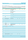
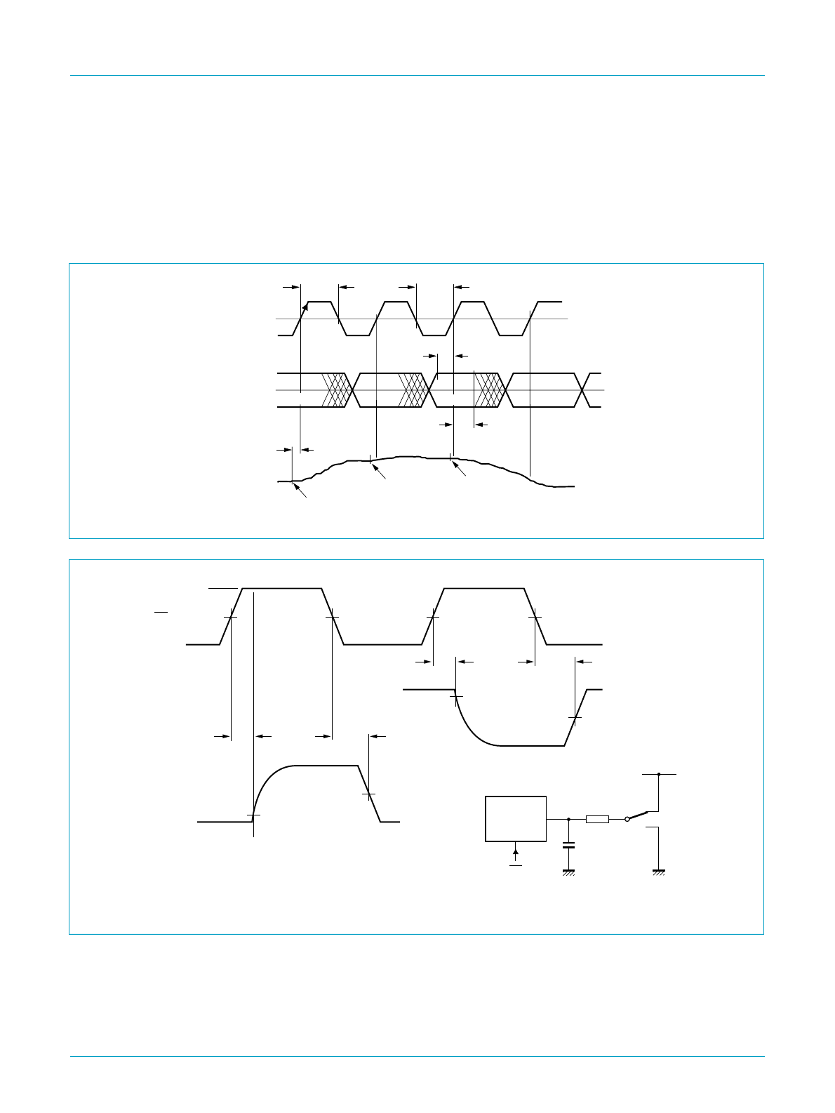
Fig 11. Data timing diagram.
t
d(s)
sample N + 1
sample N + 2
sample N
CKADCO
n
FCE475
50 % = 1.4 V
1.4 V
2.4 V
0.4 V
V
in
DATA
R0 to R7, ROR
G0 to G7, GOR
B0 to B7, BOR
t
d(o)
t
h(o)
t
CPH
t
CPL
I
n − 1
I
n + 1
I
n + 2
I
n
f
OE
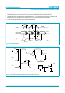
= 100 kHz; switch S1 connected to V
CCD
for t
dLZ
and t
dZL
; switch S1 connected to GND for t
dHZ
and t
dZH
.
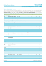
Fig 12. Timing diagram and test conditions of 3-state output delay time.
handbook, full pagewidth
output
data
output
data
OE
50%
50%
50%
10%
90%
LOW
TDA8752B
LOW
HIGH
HIGH
t
dZH
t
dZL
t
dHZ
V
CCD
t
dLZ
3.3 kΩ
FCE476
S1
OE
V
CCD
10 pF