


Philips Semiconductors
TDA8752B
Triple high-speed Analog-to-Digital Converter 110 Msps
Product specification Rev. 03 — 21 July 2000 2 of 38
9397 750 07338
© Philips Electronics N.V. 2000. All rights reserved.
■ Power-down mode
■ Possibility to use up to four ICs in the same system when using the I
2
C-bus
interface, or more when using the 3-wire serial bus interface
■ 1.1 W power dissipation.
3. Applications
■ RGB high-speed digitizing
■ LCD panels drive
■ LCD projection systems
■ VGA and higher resolutions
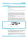
■ Using two ICs in parallel, a higher display resolution can be obtained: 200 MHz
pixel frequency.
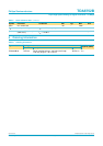
4. Quick reference data
Table 1: Quick reference data
Symbol Parameter Conditions Min Typ Max Unit
V
CCA
analog supply voltage for R, G and B channels 4.75 5.0 5.25 V
V
DDD
logic supply voltage for I
2
C-bus and 3-wire
serial bus
4.75 5.0 5.25 V
V
CCD
digital supply voltage 4.75 5.0 5.25 V
V
CCO
output stages supply voltage for R, G and B channels 4.75 5.0 5.25 V
V
CCA(PLL)
analog PLL supply voltage 4.75 5.0 5.25 V
V
CCO(PLL)
output PLL supply voltage 4.75 5.0 5.25 V
I
CCA
analog supply current − 120 − mA
I
DDD
logic supply current for I
2
C-bus and 3-wire − 1.0 − mA
I
CCD
digital supply current − 40 − mA
I
CCO
output stages supply current f
clk
= 110 MHz; ramp input − 26 − mA
I
CCA(PLL)
analog PLL supply current − 28 − mA
I
CCO(PLL)
output PLL supply current − 5 − mA
f
clk
clock frequency −−110 MHz
f
ref(PLL)
PLL reference clock
frequency
15 − 280 kHz
f
VCO
VCO output clock frequency 12 − 110 MHz
INL DC integral non-linearity from analog input to digital
output; full-scale; ramp
input; f
clk
= 110 MHz
−±0.5 ±1.5 LSB
DNL DC differential non-linearity from analog input to digital
output; full-scale; ramp
input; f
clk
= 110 MHz
−±0.5 ±1.0 LSB
∆G
amp
/∆T amplifier gain stability as a
function of temperature
V
ref
= 2.5 V with
100 ppm/°C maximum
−−200 ppm/°C
B amplifier bandwidth −3 dB; T
amb
=25°C 250 −−MHz
t
set
settling time of the ADC block
plus AGC
input signal settling
time <1 ns; T
amb
=25°C
−−6ns