


Philips Semiconductors
TDA8752B
Triple high-speed Analog-to-Digital Converter 110 Msps
Product specification Rev. 03 — 21 July 2000 24 of 38
9397 750 07338
© Philips Electronics N.V. 2000. All rights reserved.
10. Limiting values
11. Thermal characteristics
12. Characteristics
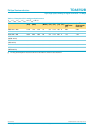
Table 15: Limiting values
In accordance with the Absolute Maximum Rating System (IEC 60134).
Symbol Parameter Conditions Min Max Unit
V
CCA
analog supply voltage −0.3 +7.0 V
V
CCD
digital supply voltage −0.3 +7.0 V
V
DDD
logic supply voltage −0.3 +7.0 V
V
CCO
output stages supply voltage −0.3 +7.0 V
∆V
CC
supply voltage differences
V
CCA
− V
CCD
−1.0 +1.0 V
V
CCO
− V
CCD
; V
CCO
− V
DDD
−1.0 +1.0 V
V
CCA
− V
DDD
; V
CCD
− V
DDD
−1.0 +1.0 V
V
CCA
− V
CCO
−1.0 +1.0 V
V
i(RGB)
RGB input voltage range referenced
to AGND
−0.3 +7.0 V
I
o
output current − 10 mA
I
I(OE)
input current pin OE − 1.0 mA
I
I(PWDWN)
input current pin PWDWN − 1.0 mA
T
stg
storage temperature −55 +150 °C
T
amb
ambient temperature 0 70 °C
T
j
junction temperature − 150 °C
Table 16: Thermal characteristics
Symbol Parameter Conditions Value Unit
R
th(j-a)
thermal resistance from junction to
ambient
in free air 52 K/W
Table 17: Characteristics
V
CCA
=V
11
(or V
19
,V
27
or V
99
) referenced to AGND (V
13
,V
21
,V
29
or V
96
) = 4.75 to 5.25 V; V
CCD
=V
95
referenced to DGND
(V
86
) = 4.75 to 5.25 V; V
DDD
=V
40
referenced to V
SSD
(V
41
) = 4.75 to 5.25 V; V
CCO
=V
59
(or V
69
,V
79
or V
85
) referenced to
OGND (V
48
,V
60
,V
70
or V
82
) = 4.75 to 5.25 V; AGND, DGND, OGND and V
SSD
connected together; T
amb
= 0 to 70
°
C; typical
values measured at V
CCA
=V
DDD
=V
CCD
=V
CCO
= 5 V and T
amb
=25
°
C; unless otherwise specified.
Symbol Parameter Conditions Min Typ Max Unit
Supplies
V
CCA
analog supply voltage 4.75 5.0 5.25 V
V
CCD
digital supply voltage 4.75 5.0 5.25 V
V
DDD
logic supply voltage 4.75 5.0 5.25 V
V
CCO
output stages supply
voltage
4.75 5.0 5.25 V
I
CCA
analog supply current − 120 − mA