


Philips Semiconductors
TDA8752B
Triple high-speed Analog-to-Digital Converter 110 Msps
Product specification Rev. 03 — 21 July 2000 27 of 38
9397 750 07338
© Philips Electronics N.V. 2000. All rights reserved.
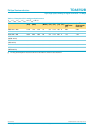
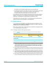
DNL DC differential non linearity from IC analog input to digital
output; ramp input;
f
clk
= 110 MHz
−±0.5 ±1.0 LSB
ENOB effective number of bits from IC analog input to digital
output; 10 kHz sine wave
input; ramp input;
f
clk
= 110 MHz
[1]
− 7.4 − bits
Signal-to-noise ratio
S/N signal-to-noise ratio maximum gain; f
clk
= 110 MHz − 45 − dB
minimum gain; f
clk
= 110 MHz − 44 − dB
Spurious free dynamic range
SFDR spurious free dynamic
range
maximum gain; f
clk
= 110 MHz − 60 − dB
minimum gain; f
clk
= 110 MHz − 60 − dB
Clock timing output (CKADCO, CKBO and CKAO)
η
ext
ADC clock duty cycle 100 MHz output 45 50 55 %
f
clk
clock frequency −− 110 MHz
Clock timing input (CKEXT)
f
clk
clock frequency −− 110 MHz
t
CPH
clock pulse width HIGH 3.6 −−ns
t
CPL
clock pulse width LOW 4.5 −−ns
t
d(CLKO)
delay from CKEXT to
CKADCO
INV set to LOW 9.5 10.1 10.7 ns
INV set to HIGH − 10.1 +
1
⁄
2
t
clk
− ns
∆t-t
d(CLKO)
time difference between
samples
when operated in the same
supply and temperature
conditions
− 0.1 0.3 ns
Data timing (see Figure 11); f
clk
= 110 MHz; C
L
=10pF;
[2]
t
d(s)
sampling delay time referenced to CKADCO −− − ns
t
d(o)
output delay time −−2 −1.5 ns
t
h(o)
output hold time 1.5 2.3 − ns
3-state output delay time (see Figure 12)
t
dZH
output enable HIGH − 12 − ns
t
dZL
output enable LOW − 10 − ns
t
dHZ
output disable HIGH − 50 − ns
t
dLZ
output disable LOW − 65 − ns
PLL clock output
V
OL
LOW-level output voltage I
o
=1mA − 0.3 0.4 V
V
OH
HIGH-level output voltage I
o
= −1 mA 2.4 3.5 − V
I
OL
LOW-level output current V
OL
= 0.4 V − 2 − mA
I
OH
HIGH-level output current V
OH
= 2.7 V −−0.4 − mA
Table 17: Characteristics
…continued
V
CCA
=V
11
(or V
19
,V
27
or V
99
) referenced to AGND (V
13
,V
21
,V
29
or V
96
) = 4.75 to 5.25 V; V
CCD
=V
95
referenced to DGND
(V
86
) = 4.75 to 5.25 V; V
DDD
=V
40
referenced to V
SSD
(V
41
) = 4.75 to 5.25 V; V
CCO
=V
59
(or V
69
,V
79
or V
85
) referenced to
OGND (V
48
,V
60
,V
70
or V
82
) = 4.75 to 5.25 V; AGND, DGND, OGND and V
SSD
connected together; T
amb
= 0 to 70
°
C; typical
values measured at V
CCA
=V
DDD
=V
CCD
=V
CCO
= 5 V and T
amb
=25
°
C; unless otherwise specified.
Symbol Parameter Conditions Min Typ Max Unit