


S3F80P5_UM_ REV1.00 CLOCK AND POWER CIRCUITS
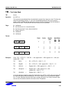
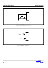
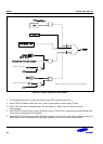
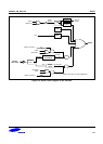
VDD
VDD
R 1
C 1 C 2
Figure 7-5. Power Circuit (VDD)
Typically, application systems have a resister and two separate capacitors across the power pins. R1 and C1
located as near to the MCU power pins as practical to suppress high-frequency noise. C2 should be a bulk
electrolytic capacitor to provide bulk charge storage for the overall system. We recommend that R1=10ohm,
C1=0.1uF and C2=100uF.
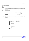
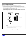
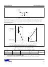
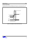
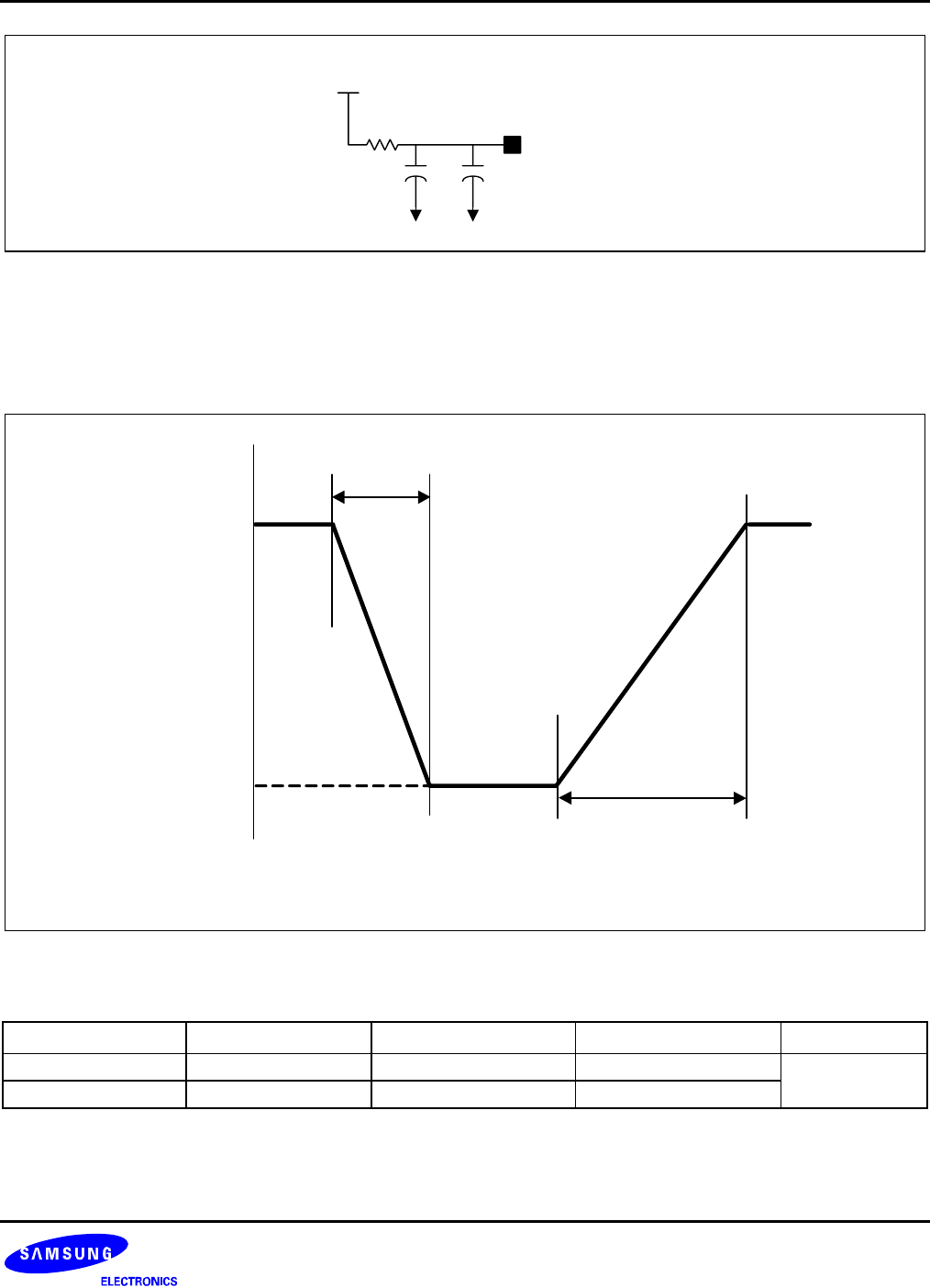
V
DD
VBAT (3.6V)
(Note 2)
VBAT (1.55V)
VF
VR
(Note1)
VF: VDD falling time should be at least 100us for stabilized IVC VDD.
VR: VDD rising time should be at least 500us for stabilized IVC VDD.
Figure 7-6. Guide Line of Chip Operating Voltage
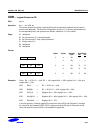
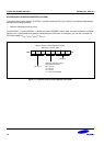
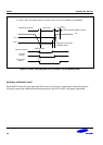
Table 7-1. Falling and Rising Time of Operating Voltage
V
DD
Slope
Min Typ Max Unit
VF 100 - -
VR 500 - -
us
NOTES:
1. In order to reduce overshoot,
VR is longer than VF
2. Since VDD=3.6V is the worst case
, IVC VDD will be stabilized when VF>=100us, VR>=500us.
7-5