


CONTROL REGISTERS S3F80P5_UM_ REV1.00
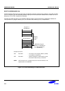
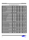
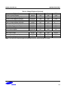
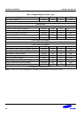
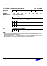
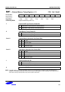
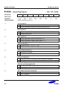
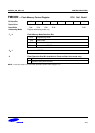
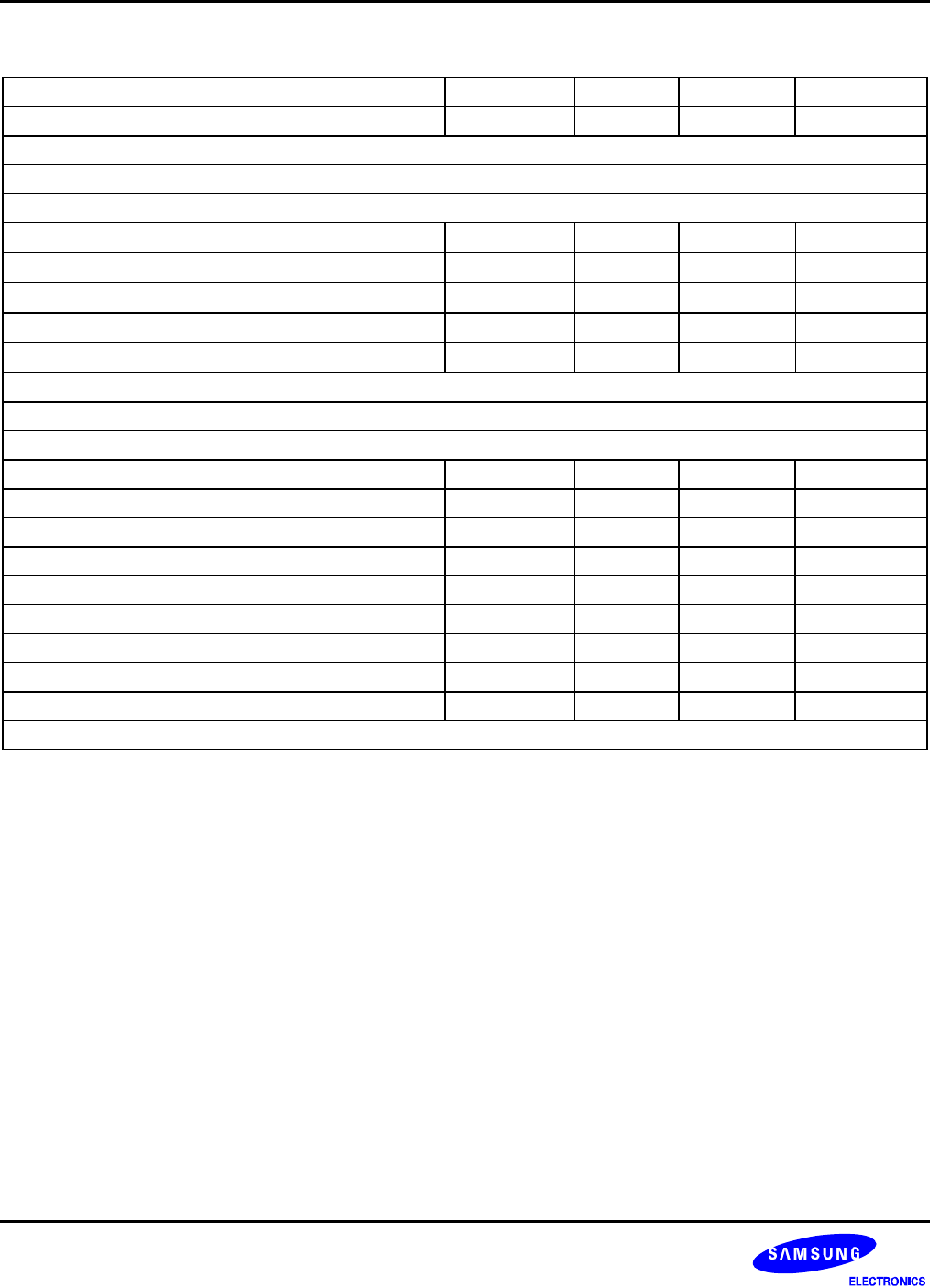
Table 4-2. Mapped Registers (Bank1, Set1)
Register Name Mnemonic Decimal Hex R/W
LVD Control Register LVDCON 224 E0 R/W
Reserved E1H
Reserved E2H
Reserved E3H
Timer 2 Counter Register (High Byte) T2CNTH 228 E4
R
(NOTE)
Timer 2 Counter Register (Low Byte) T2CNTL 229 E5
R
(NOTE)
Timer 2 Data Register (High Byte) T2DATAH 230 E6 R/W
Timer 2 Data Register (Low Byte) T2DATAL 231 E7 R/W
Timer 2 Control Register T2CON 232 E8 R/W
Location E9H is not mapped.
Location EAH is not mapped.
Location EBH is not mapped.
Flash Memory Sector Address Register (High Byte) FMSECH 236 EC R/W
Flash Memory Sector Address Register (Low Byte) FMSECL 237 ED R/W
Flash Memory User Programming Enable Register FMUSR 238 EE R/W
Flash Memory Control Register FMCON 239 EF R/W
Reset Indicating Register RESETID 240 F0 R/W
LVD Flag Selection Register LVDSEL 243 F1 R/W
PORT1 Output Mode Pull-up Enable Register P1OUTPU 244 F2 R/W
PORT2 Output Mode Selection Register P2OUTMD 245 F3 R/W
PORT3 Output Mode Pull-up Enable Register P3OUTPU 246 F4 R/W
Not mapped in address F5H to 0FFH
NOTE: You cannot use a read-only register as a destination for the instructions OR, AND, LD, or LDB.
4-4