


S3F80P5_UM_ REV1.00 S3F80P5 FLASH MCU
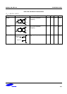
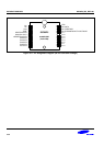
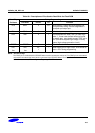
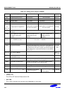
Table 18-1. Descriptions of Pins Used to Read/Write the Flash ROM
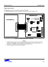
Main Chip During Programming
Pin Name Pin Name Pin No. I/O Function
P0.0
SDAT 5 I/O Serial data pin. Output port when reading and
input port when writing. Can be assigned as a
Input/push-pull output port.
P0.1 SCLK 6 I Serial clock pin. Input only pin.
TEST TEST 4 I Tool mode selection when TEST pin sets Logic
value ‘1’. If user uses the flash writer tool mode
(ex.spw2+ etc.), user should connect TEST pin to
VDD. (S3F80P5 supplies high voltage 12.5V by
internal high voltage generation circuit.)
nRESET nRESET 7 I Chip Initialization
V
DD
,
V
SS
V
DD
,
V
SS
24,
1
– Power supply pin for logic circuit. VDD should be
tied to +3.3V during programming.
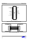
NOTE: Test Pin Voltage
The TEST pin on socket board for OTP/MTP writer must be connected to Vdd (3.3V). The TEST pin on socket board
must not be connected Vpp(12.5V) which is generated from OTP/MTP Writer. So the specific socket board for
S3F80P5 must be used, when writing or erasing using OTP/MTP writer.
18-3