


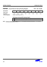


S3F80P5_UM_ REV1.00 CONTROL REGISTERS
NOTES:
1. The port 3 data register, P3, at location E3H, set1, bank0, contains seven bit values which correspond to the following
Port 3 pin functions (bit 6 is not used for the S3F80P5)
a. Port3, bit 7: carrier signal on (“1”) or off (“0”).
b. Port3, bit 1,0: P3.1/REM/T0CK pin, bit 0: P3.0/T0PWM/T0CAP/T1CAP pin.
2. The alternative function enable/disable are enabled in accordance with function selection bit (bit5 and bit2).
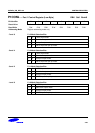
3. Following Table is the specific example about the alternative function and pin assignment according to the each bit
control of P3CON in 24 pin package.
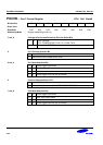
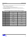
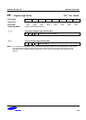
Table 4-3. Each Function Description and Pin Assignment of P3CON in 24 Pin Package
P3CON
Each Function Description and Assignment to P3.0−P3.3
B5 B4 B3 B2 B1 B0 P3.0 P3.1
0 x x 0 x x Normal I/O Normal I/O
0 x x 1 0 0 T0_CAP/T1_CAP Normal I/O
0 x x 1 1 1 T0_CAP/T1_CAP Normal I/O
0 x x 1 0 1 T0PWM Normal I/O
0 x x 1 1 0 T0PWM Normal I/O
1 0 0 0 x x Normal I/O T0CK
1 1 1 0 x x Normal I/O T0CK
1 0 1 0 x x Normal I/O REM
1 1 0 0 x x Normal I/O REM
1 0 0 1 0 0 T0_CAP/T1_CAP T0CK
1 1 1 1 1 1 T0_CAP/T1_CAP T0CK
1 0 1 1 0 1 T0PWM REM
1 1 0 1 1 0 T0PWM REM
1 0 0 1 0 1 T0PWM Normal Input
1 1 1 1 1 0 T0PWM Normal Input
1 0 1 1 0 0 T0_CAP/T1_CAP REM
1 1 0 1 1 1 T0_CAP/T1_CAP REM
4-33