


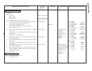

KL-W7000/W9000
RM-Y980
KL-W7000/W9000
RM-Y980
KL-W7000/W9000
RM-Y980
KL-W7000/W9000
RM-Y980
– 52 –– 51 –
– 54 –
– 53 –
MEMO MEMO
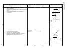
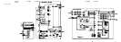
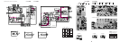
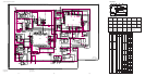
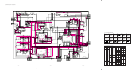
4-2. CIRCUIT BOARDS LOCATION
C
TB
TA
HB
HA
Power block
GA
G
A
BB
U
K
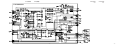
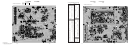
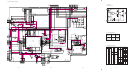
4-3. SCHEMATIC DIAGRAMS AND PRINTED WIRING BOARDS
Note:
• All capacitors are in µF unless otherwise noted. (pF: µµF)
Capacitors without voltage indication are all 50 V.
• Indication of resistance, which does not have one for rating
electrical power, is as follows.
Pitch: 5 mm
Rating electrical power 1/4 W (CHIP : 1/10 W)
• All resistors are in ohms.
•
f : nonflammable resistor.
• Ï : fusible resistor.
•
¢ : internal component.
•
p : panel designation, and adjustment for repair.
• All variable and adjustable resistors have characteristic curve B,
unless otherwise noted.
•
e : earth-ground.
• E : earth-chassis.
• All voltages are in V.
• Readings are taken with a 10 M digital multimeter.
• Readings are taken with a color-bar signal input.
• Voltage variations may be noted due to normal production
tolerances.
*
: Can not be measured.
• Circled numbers are waveform references.
•
s : B + bus.
• S : B – bus.
•
m : Signal path.
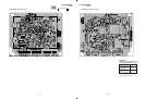
Reference information
RESISTOR : RN METAL FILM
: RC SOLID
: FPRD NONFLAMMABLE CARBON
: FUSE NONFLAMMABLE FUSIBLE
: RW NONFLAMMABLE WIREWOUND
: RS NONFLAMMABLE METAL OXIDE
: RB NONFLAMMABLE CEMENT
COIL : LF-8L MICRO INDUCTOR
CAPACITOR : TA TANTALUM
: PS STYROL
: PP POLYPROPYLENE
: PT MYLAR
: MPS METALIZED POLYESTER
: MPP METALIZED POLYPROPYLENE
: ALB BIPOLAR
: ALT HIGH TEMPERATURE
: ALR HIGH RIPPLE
Note: The components identified by shading and mark
¡ are critical for safety. Replace only with part
number specified.
Note: Les composants identifiés per un tramé et une
marque ¡ sont critiques pour la sécurité. Ne les
remplacer que par une pièce portant le numéro
spécifié.
G
D
S
B1 E1C2
B2 C1E2
2
3
4
5
6
7
8
9
0
!¡
!™
!¢
!§
!¶
!•
–
1
G
D
S
B2 E2C1
B1 C2E1
B2 E2C1
B1 C2E1
B2 E2C1
B1 C2E1
!ª
B1 E1
E2
C1(B2)C2
@º
B1
E2
C1C2
@™
(B2)
E1
(B2)
E1
E2
B1
C2C1
@¡
B1
E1
C2
B2
C1
E2
G
S
S
D
G
D
B1
E1
C2
B2
C1
E2
B1
E2
C2C1(B2)
E2
B1
C1
C2E1(B2)
C2
B1
C1
E2E1(B2)
C2
B1
C1
E2
B2
E1
C2
Ver.1.4
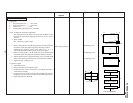
Transistor
(FET)
Transistor
Transistor
Transistor
Transistor
Transistor
Transistor
Transistor
Transistor
Transistor
Discrete semiconductot
(
Chip semiconductors that are not actuall
y
used are included.
)
Diode
Diode
Diode
Diode
Diode
Diode
Diode
Diode
Diode
Source
Source
Anode
Anode
(NC)
(NC)
Cathode
Anode
Cathode
Common
Cathode
Cathode
Common
Cathode
Cathode
Common
Common
Common
Common
Cathode
Anode
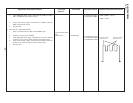
Base
Emitter
Collector
Base
Emitter
Collector
Drain
Gate
Gate
Drain
Device Printed symbol Terminal name
Circuit
Terminal name of semiconductors in silk screen
printed circuit ( )
Anode
Anode
Anode Cathode
Anode Anode
Cathode
!£
Transistor
(FET)
Transistor
(FET)
!∞
Emitter
Collector
Base
Transistor
Source
Gate
Drain
*