


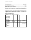

39
the status of the receive operation is double
buffered in order to retain the results of the first
reception for analysis by the processor,
therefore the information will remain in the
Status Register until the "Clear Receive
Interrupt" command is issued. Note that the
interrupt will remain active until the "Clear
Receive Interrupt" command is issued, and the
second interrupt will be stored until the first
interrupt is acknowledged. A minimum of
200nS interrupt inactive time interval between
interrupts is guaranteed.
The second reception will occur as soon as a
second packet is sent to the node, as long as
the second "Enable Receive to Page fnn"
command was issued. The operation is as if a
new "Enable Receive to Page fnn" command
has just been issued. After the first Receive
status bits are cleared, the Status Register will
again be updated with the results of the second
reception and a second interrupt resulting from
the second reception will occur.
In the COM20020, the Receive Inhibit (RI) bit of
the Interrupt Mask Register now masks only the
TRI bit of the Status Register, not the RI bit as
in the non-chaining mode. Since the TRI bit is
only set upon reception of a packet (not by
RESET), and since the TRI bit may easily be
reset by issuing a "Clear Receive Interrupt"
command, there is no need to use the RI bit of
the Interrupt Mask Register to mask interrupts
generated by the TRI bit of the Status Register.
In Command Chaining mode, the "Disable
Receiver" command will cancel the oldest
reception, unless the reception has already
begun. If both receptions should be canceled,
two "Disable Receiver" commands should be
issued.
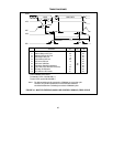
RESET DETAILS
Internal Reset Logic
The COM20020 includes special reset circuitry
to guarantee smooth operation during reset.
Special care is taken to assure proper operation
in a variety of systems and modes of operation.
The COM20020 contains digital filter circuitry
and a Schmitt Trigger on the nRESET IN signal
to reject glitches in order to ensure fault-free
operation.
The COM20020 supports two reset options;
software and hardware reset. A software reset
is generated when a logic "1" is written to bit 7
of the Configuration Register. The device
remains in reset as long as this bit is set. The
software reset does not affect the
microcontroller interface modes determined
after hardware reset, nor does it affect the
contents of the Address Pointer Registers, the
Configuration Register, or the Setup Register. A
hardware reset occurs when a low signal is
asserted on the nRESET IN input. The
minimum reset pulse width is 3.2µs. This pulse
width is used by the internal digital filter, which
filters short glitches to allow only valid resets to
occur.
Upon reset, the transmitter portion of the device
is disabled and the internal registers assume
those states outlined in the Internal Registers
section.
After the nRESET IN signal is removed the user
may write to the internal registers. Since writing
a non-zero value to the Node ID Register wakes
up the COM20020 core, the Setup Register
should be written before the Node ID Register.
Once the Node ID Register is written to, the
COM20020 reads the value and executes two
write cycles to the RAM buffer. Address 0 is
written with the data D1H and address 1 is
written with the Node ID. The data pattern D1H
was chosen arbitrarily, and is meant to provide
assurance of proper microsequencer operation.