


4
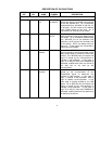
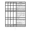
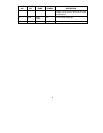
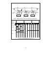
DESCRIPTION OF PIN FUNCTIONS
DIP PIN
NO.
PLCC PIN
NO.
NAME
SYMBOL DESCRIPTION
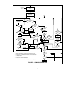
MICROCONTROLLER INTERFACE
1-3 1-3 Address
0-2
A0/nMUX,
A1,A2/ALE
Input. On a non-multiplexed bus, these
signals are directly connected to the low bits
of the host address bus. On a multiplexed
address/data bus, A0/nMUX is tied low, A1
is left open, and A2 is tied to the Address
Latch Enable signal of the host. A1 is
connected to an internal pull-up resistor.
4-11 4-6,8-12 Data 0-7 AD0-AD2,
D3-D7
Input/Output. On a non-multiplexed bus,
these signals are used as the data lines for
the device. On a multiplexed address/data
bus, AD0-AD2 act as the address lines
(latched by ALE) and as the low data lines
for the device. D3-D7 are always used for
data only. These signals are connected to
internal pull-up resistors.
23 27 nRead/nData
nStrobe
nRD/nDS Input. On a 68XX-like bus, this active low
signal is issued by the microcontroller as the
data strobe signal to strobe the data onto
the bus. On a 80XX-like bus, this active low
signal is issued by the microcontroller to
indicate a read operation. In this case, a
logic "0" on this pin, when the COM20020 is
accessed, enables data from the device to
the data bus to be read by the
microcontroller.
22 26 nWrite/
Direction
nWR/DIR Input. On a 68XX-like bus, this signal is
issued by the microcontroller as the
Read/nWrite signal to determine the
direction of data transfer. In this case, a
logic "1" selects a read operation, while a
logic "0" selects a write operation. In this
case, data is actually strobed by the nDS
signal. On an 80XX-like bus, this active low
signal is issued by the microcontroller to
indicate a write operation. In this case, a
logic "0" on this pin, when the COM20020 is
accessed, enables data from the data bus to
be written to the device.