VXI Technology, Inc.
12 SVM2608 Introduction
1x, 2x, 5x, 10x
LPF
FILTER
attn
gain1
gain0
CHn +I
CHn+
CHn–
CHnI–
ADC
16
DAC
TRIG
FORCE
POL
DAC
EXT TRIG
EXT TRIG
GLUE LOGIC
CHANNEL 1 TRIG
DATA
ADDRESS
CONTROLS
CHANNEL 0
TRIG
DATA &
CONTROLS
CHANNEL 2 TRIG
CHANNEL 3 TRIG
μP
+
–
÷ 1
÷ 10
+
–
+
–
MEMORY
VME INTERFACE
DATA & CONTROL
VME BACKPLANE
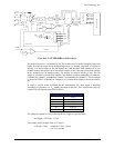
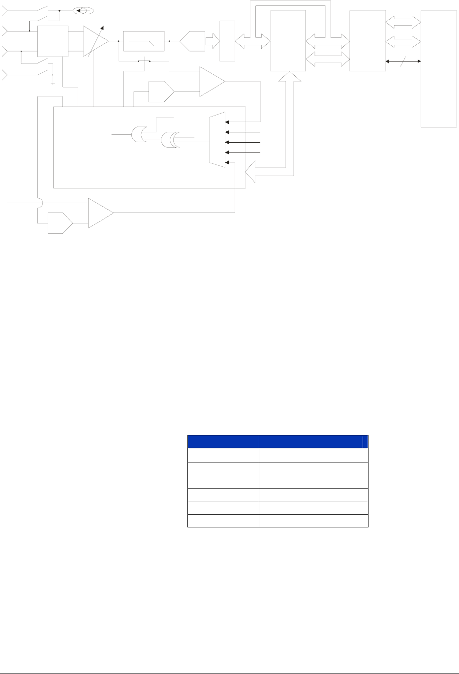
FIGURE 1-1: SVM2608 BLOCK DIAGRAM
The acquisition process is controlled by two FPGAs that allow for greater flexibility along with
higher speed and precision during the digitizing process. As the data is digitized, it is placed in
memory. It is then available to the user through the VME interface. Each channel has its own
channel memory that can store up to one million samples of data. This data is also made available
to the microprocessor for data processing. The samples are stored as words (16 bits). The first
sample of a channel is located at the channel’s base address at Offset 0 (0x000000 for Channel 0,
0x200000 for Channel 1, 0x400000 for Channel 2 and 0x600000 for Channel 3). The next sample
is located at Offset 2 (0x000002 for Channel 0, etc.) and the third sample is located at Offset 4,
etc.
In order to provide better resolution for the measurement, the input signal is amplified
accordingly to generate a ±10 V
P-P
signal at the input of the ADC. Thus, on different scales, the
weight of a bit of digitized data will be different:
SCALE (V) Bit Weight (μV/count)
1 30.518
2 61.035
5 152.588
10 305.176
20 610.352
50 1525.879
The following equation is used to determine the bit weight at a specified scale:
Bit Weight = Full Scale / 32,768
For example, the Bit Weight of the 10 V range is:
10.0 volts / 32768 = 0.0003051757813 V/count
≈ 305.176 µV/count


