VXI Technology, Inc.
32 SVM2608 Programming
The binary values are then converted into a hexadecimal format:
Binary
Hexadecimal
0000 0000 0110 0010 0x0062
This determines the data value required for the aforementioned settings.
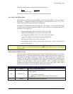
ACCESSING THE REGISTERS
With both D16 and D32 data transfer available, the user can write either 16 or 32 bits of data to
the registers. To change the settings of the module, it is only necessary to write a 16- or 32-bit
integer to the specified register with the new configuration.
All registers, as defined in the following section, are 16-bit registers. A 32-bit write can be made
to registers that are located in consecutive addresses. The consecutive 16-bit registers that can be
accessed as 32-bit registers are:
Sample Rate Register (0x0C, 0x34, 0x5C, 0x84, 0xAC, 0xD4)
Sample Points Register (0x10, 0x38, 0x60, 0x88, 0xB0, 0xD8)
Pre-Trigger Points Register (0x14, 0x3C, 0x64, 0x8C, 0xB4, 0xDC)
Trigger Delay Register (0x18, 0x40, 0x68, 0x90, 0xB8, 0xE0)
FIFO data (0x24, 0x4C, 0x74, 0x9C, 0xC4, 0xEC)
Result Register (0x28 & 0x2C, 0x50 & 0x54, 0x78 & 0x7C, 0xA0 & 0xA4, 0xC8 &
0xCB, 0xF0 & 0xF4)
NOTE Reading 32 bits from a 16-bit register may generate a BERR on the VME bus.
Writing 32 bits to a 16-bit register may generate a BERR on the VME bus or may corrupt data in
another register.
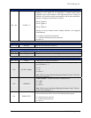
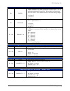
DESCRIPTION OF REGISTERS
The following pages describe the registers found in the SVM2608 Register Map for A32 address
space that starts at 0x00C0000. When multiple channels registers have the same functions, the
offsets appear in parenthesis separated by commas with Channel 0 being listed first, followed by
Channel 1, etc. For example, the description used by the Control Register Bit is applicable to all
six channels at offsets 0x08 for Channel 0, 0x30 for Channel 1, 0x58 for Channel 2 and 0x80 for
Channel 3, 0xA8 for Channel 4 and 0xD0 for Channel 5. This is indicated in the register
description by using the following notation: (0x08, 0x30, 0x58, 0x80, 0xA8, 0xD0). Unless
otherwise noted, register descriptions apply to all channels (Channels 0 – 5).
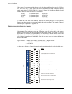
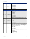
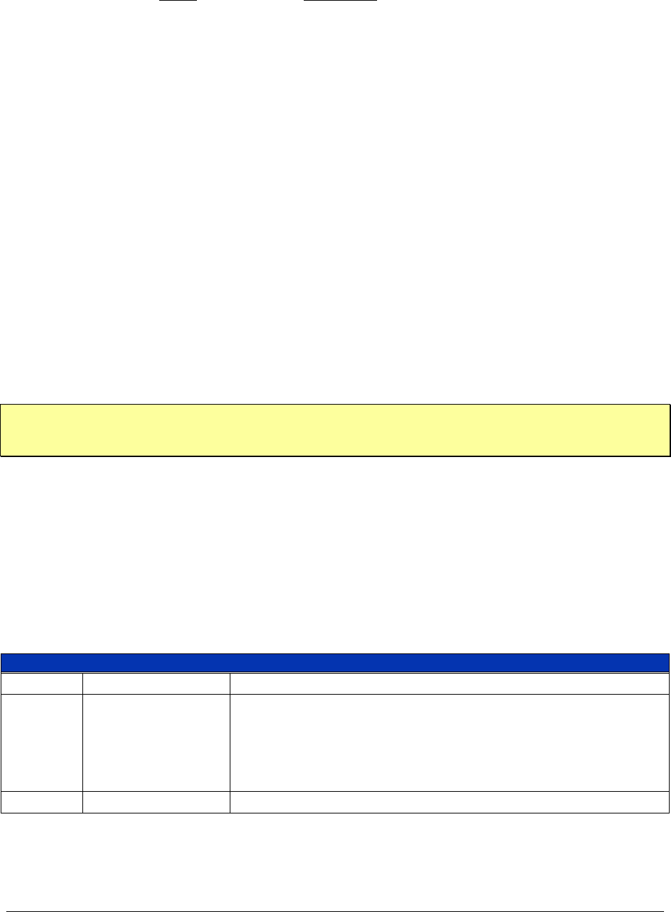
Reset, Sys Fail Control, Interrupt Levels Register (0x00) — Read & Write
D15 Unused This bit is reserved for future use.
D14 SYSFAILCTL
System Fail Control - This bit controls whether or not the sysfail line
will be masked.
0 = Card can assert sysfail line.
1 = Sysfail line is masked and card cannot assert sysfail line.
P
on
state = 0
D13 – D3 Unused These bits are reserved for future use.


