


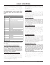

CIRCUIT DESCRIPTIONS
PV154 - 923-03506 3-8 ZP26/28 - SERVICING
30Kv HV
30,000 volts DC supplied to the CRTs anodes.
TO DEFLECTION YOKES
Horizontal and Vertical deflection wave forms driving
the deflection yokes.
MAGIC SWITCH
Output from the DAC1 (I006 pin 7) when the customer
selects HD FOCUS from the customer’s menu. This ener-
gizes HD FOCUS, (Magic Focus).
SERVICE ONLY SWITCH
Enters the Digital Convergence Adjustment Mode,
(DCAM).
HORIZONTAL DRIVE CIRCUIT DESCRIPTION:
When B+ arrives at the Rainforest IC IC01 pin (19), hori-
zontal drive is output from pin (26). The drive signal is
routed through the connector PSD2 pin 5 to the Hori-
zontal Driver Transistor Q751. This transistor switches
the ground return for pin (8) of the Driver transformer
(T751). 28 volts is supplied to pin (5) and this switch-
ing allows EMF to develop. As this signal collapses, it
creates a pulse on the output pin of (T751) at pin (4)
to the base of the Deflection Horizontal output transis-
tor Q777.
Two transistors monitor the SW +9V line, Q707 and Q708.
When the set is turned off, the H. Drive signal from
IC01 could stop too soon. If this were to happen, the
Horizontal output transistor Q777 would be damaged.
To prevent this, if the SW +9V line drops, Q707 senses
this because its base voltage drops. The base of Q708
rises and turns on, grounding the output from the H.
Drive Transistor Q709.
Q709 transistor switches the primary windings of the
Deflection Transformer T752.
T702 TRANSFORMER PRODUCES THE FOLLOWING OUT-
PUT PULSES;
••
••
• Deflection Pulse from pin (7): This pulse is used by:
1. X-Ray Protect through D707: This signal is
monitored by the X-Ray Protect circuit to place
the power supply into shut down if the Deflec-
tion circuit doesn’t operate.
2. The Dynamic Focus OUT Circuit PWB through
PDK4 connector pin 5: A Dynamic Focus wave-
form, (Horz. Parabola) is created. This is a para-
bolic waveform that is superimposed upon the
static focus voltage to compensate for beam
shape abnormalities which occur on the out-
side edges of the screen because the beam has
to travel further to those locations.
3. 1100V Generation circuit through D711, D712
and the connector PDF1 pin 1.
This is the Dynamic Focus output voltage.
· +28V, -26V and RETRACE PULSE +28V and -28V: The
+28V and the -28V are routed to the Deflection trans-
former T752. They enter the transformer as a pure DC
voltage then a 7.5V P/P horizontal pulse is added to
the DC voltage and leave as +28P and M28P. From
here these voltages are routed to the Convergence
output section and they are rectified. They become
+33V and -33V respectively. This process prevents
the need for another power supply. (Note: the M stands
for Minus voltage.)
H. BLK GENERATED FROM PIN 7:
The Horizontal Pulse is also routed to the Horizontal
Blanking generation transistor Q706. This transistor
generates the 13V P/P called H Blk. This signal goes to
the following circuits:
· To pin the PSD2 connector pin 7 to pin (24) of IC01
as FBP In. Here this signal is used as a comparison
signal. It is compared to the reference signal com-
ing in at pin (15) Horizontal Sync. If there are any
differences between these two signals, the output
Drive signal from pin (26) is corrected.
NOTE: When a 1080i signal is input through component
inputs, the Rainforest IC detects this as well and
outputs the Vertical Squeeze (V. Squ) signal from
pin (36). The Reference signal for Horizontal Sync
now becomes the Y input from component, pin (8).
· To the Convergence circuit for correction waveform
generation.
· Sweep Loss Circuit (QN01) to shut off the CRTs if
Horizontal deflection is lost.
· Through the connector PSD2 pin (7): The H Blk sig-
nal is routed from here to the Signal PWB to be used
by different circuits.
The Microprocessor uses this signal for OSD positioning
and for Station Detection during Auto programming
within the coincidence detector.
The PinP unit uses this signal for switching purposes.
Like the read/write clock, positioning, etc…
· The Horizontal Blanking signal H Blk from Q706 is
also sent to the High Voltage Driver IC IH01 pin (3).
This IC uses this signal as its reference signal to
produce the High Voltage Drive waveform output from
pin (1). This output is routed to the driver transis-
tors, QH02. Then to the High Voltage Horizontal
Output Transistor QH01. This transistor switches the
primary of the Flyback transformer TH01. Deflection
B+ 115V2 is sent through pin (9) and output pin
(10) to the collector of the Horizontal Output Tran-
sistor QH01.