CIRCUIT DESCRIPTIONS
PV154 - 923-03506 3-9 ZP26/28 - SERVICING
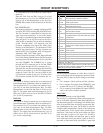
A sample of the High Voltage is output from the Flyback
transformer TH01 pin (12). This voltage is sent to pin
(9) of the High Voltage Driver IC IH01. This voltage is
compared to the reference voltage available at pin (12).
If there is a difference between the two voltages, an
error voltage is generated and output from pin (10)
and input again at pin (11) where it manipulates the
PWM (Pulse Width Modulation) signal producing the
Horizontal Drive signal output from pin (1).
The error signal from pin (10) is also sent to the Side
Pin Cushion circuit through (R752). This signal ma-
nipulates the amount of pin cushion correction depen-
dent upon the amount of High Voltage error voltage
detected by the Side Pin Cushion op-amp (I701) at pin
(3).
It’s important to notice that the High Voltage circuit
can not function without the Horizontal Deflection cir-
cuit providing a drive signal.
GENERAL INFORMATION:
The deflection circuit differs from conventional prod-
ucts. It utilizes two horizontal output circuits. One for
Deflection and one for High Voltage. There are many
terms around the Horizontal circuit that are not shown
on the Diagram. Some of these terms are explained first:
The key component in the Sweep Loss Detection circuit
is QN02. This transistor is normally biased off. When
the base becomes more negative, it will be turned on,
causing the SW +11V to be applied to two different
circuits, the Spot circuit and the High Voltage Drive
circuit.
SPOT CIRCUIT
When QN02 is turned on, the SW +11V will be applied to
the anode of DN11, forward biasing it. This voltage will
then pass through DN11. It will then be clamped by
DN12, and arrive at pin 3 of PSD2. It will then be di-
rected to the Signal PWB where it will activate the Video
Mute circuitry Q023 - Q021. This is done to prevent
CRT burns.
Another input to this circuit is pin 4 of PSD2 called
“CUT OFF”. This will activate when accessing certain
adjustment parameters in the service mode; i.e. turn-
ing off vertical drive for making CRT drive or cut-off
adjustments. When Vertical Drive is defeated, the Verti-
cal Sweep loss circuit would activate. Cut Off is routed
to QN06 to “inhibit” the Spot line from activating and
shutting off the CRTs.
HIGH VOLTAGE DRIVE CIRCUIT
When QN02 is turned on, the SW +11V will also be routed
through RN15 and DN09 and applied to the High Volt-
age Drive IC IH01 at pin 14. When this occurs, the IC
will stop generating the drive signal that is used to
produce High Voltage via QH02, the High Voltage Driver.
Again, this is done to prevent CRT burn, especially dur-
ing sweep loss.
CONCERNING QN02
There are several factors that can affect the operation
of QN02: namely loss of vertical or horizontal blanking
and spot killer or spot protect from a shutdown in the
deflection power supply.
Loss of Vertical Blanking (V Blk)
The Vertical pulse at the base of QN05 switches QN05
on and off at the vertical rate. This discharges CN03
sufficiently to prevent the base of QN04 from going
high to turn it on and activate QN02.
When the 24 Vp/p positive vertical blanking pulse is
missing from the base of QN05, it will be turned off,
which will cause the collector to go high because CN03
charges up through RN11. This in turn will cause QN04
to turn on because its base pulls up high, creating an
increase of current flow from emitter to collector and
up through RN08, (which is located across the emitter
base junction of QN02), to the SW +11V supply. This
increase of current flow through RN08 will bias on QN02
and the events described in “Spot Circuit Activation”
above will occur.
Loss of Horizontal Blanking (H Blk)
The Horizontal pulse at the base of QN01 switches QN01
on and off at the horizontal rate. This discharges CN02
sufficiently to prevent the base of QN03 from going
high to turn it on and activate QN02.
When the 11.6 Vp/p positive horizontal blanking pulse
is missing from the base of QN01, it will be turned off,
which will cause the collector to go high through DN03,
RN02 and SW +11V as CN02 charges. This in turn will
cause QN03 to turn on because its base is pulled up
high when DN02 fires. When QN03 turns on, an increase
of current flow from emitter to collector, through RN07,
and up through RN08. This increase of current flow
through RN08 will bias on QN02 and the events de-
scribed in “Spot Circuit Activation” above will occur.
The Digital Convergence circuit is responsible for main-
taining proper convergence of all three colors being
produced by the CRTs. Many different abnormalities can
be quickly corrected by running HD FOCUS.
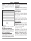
The Digital convergence Interconnect Diagram depicts
how the Digital Convergence Circuit is interfaced with
the rest of the Projection’s circuits. The main compo-
nents and/or circuits are;
• THE DIGITAL CONVERGENCE UNIT (DCU)
• INFRARED REMOTE RECEIVER
• ON SCREEN DISPLAY PATH
• CONVERGENCE OUTPUT STKs
• CONVERGENCE YOKES


