


6 F 3 B 0 3 6 4
65
(4) The Bit Strobe Output Data Area (0100H
-
0103H: 4 words)
Stores data that the DN211 outputs to slave devices in the bit strobe mode.
The ladder program for the T2/T2E/T2N writes output data in this area. The transmitting data in
the bit strobe mode is fixed at 8 bytes (64 bits).
The corresponding relation of the bits in this area and the node addresses of the slave devices is
indicated below.
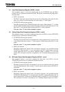
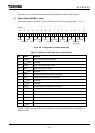
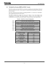
Table 4.1 Bit Strobe Output Data Area Configuration
F E D C B A 9 8 7 6 5 4 3 2 1 0
0100H 15 14 13 12 11 10 9 8 7 6 5 4 3 2 1 0
0101H 31 30 29 28 27 26 25 24 23 22 21 20 19 18 17 16
0102H 47 46 45 44 43 42 41 40 39 38 37 36 35 34 33 32
0103H 63 62 61 60 59 58 57 56 55 54 53 52 51 50 49 48
(5) The Polling Output Data Area (0080H
-
00FFH: 128 words)
Stores data that the DN211 will output to slave devices in the polling mode.
The ladder program for the T2/T2E/T2N writes output data in this area. The area has 128 words
(2048 bits) in size; unless the data size that the DN211 sends to salve devices doesn't exceed this
limit, up to 63 slave devices are connectable with one DN211.
How to allocate output data to slave devices from this area is explained in "4.4 Allocating Slave
Data to the Input/Output Data Area"
(6) The Polling/Bit Strobe Input Data Area (0000H
-
007FH: 128 words)
Stores data collected by the DN211 from the slave devices in the polling mode and bit strobe mode.
The ladder program for the T2/T2E/T2N read data from this area. The area has 128 words (2048
bits) in size; unless the data size that slave devices send to the DN211 doesn't exceed this limit, up
to 63 slave devices are connectable with one DN211.
How to allocate input data from slave devices to this area is explained in "4.4 Allocating Slave Data
to Input/Output Data Area"
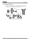
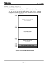
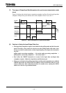
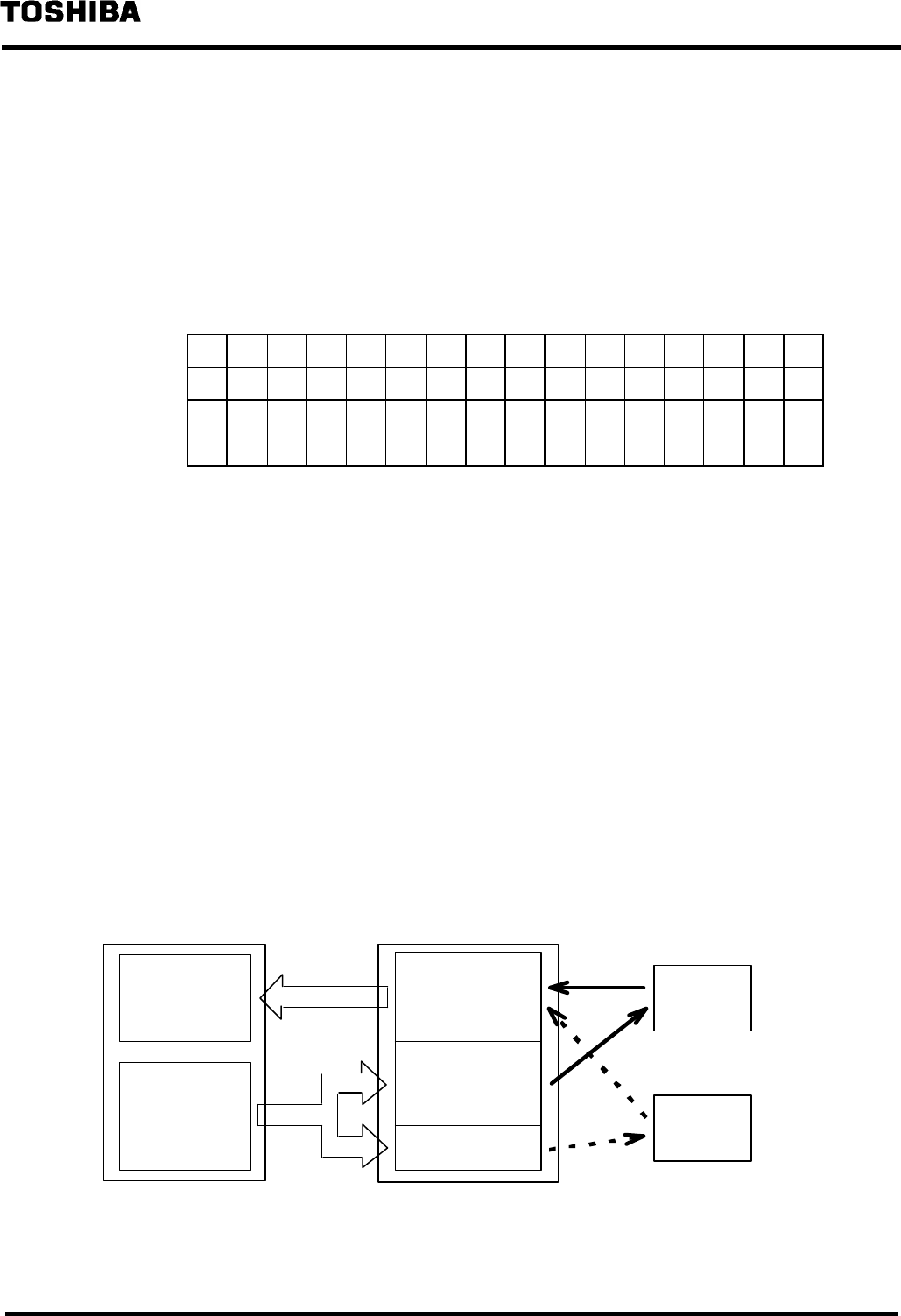
Figure 4.3. shows an overview of the output data area/input data area.
Polling
Slave
Slave
Bit strobe
Bit strobe
output data area
Polling
output data area
Polling / Bit strobe
input data area
WRITE
instr
uction
READ
instruction
Output data
register area
Input data
register area
DN211T2/T2E/T2N
Figure 4.3 Overview of Input/Output Data Area