


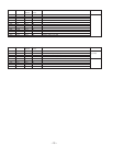

– 83 –
– 84 – – 85 – – 86 –
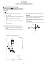
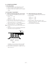
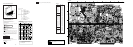
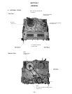
6-2. CIRCUIT BOARDS LOCATION
Note: The components identified by shading and mark B
are critical for safety. Replace only with part
nummber specified.
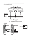
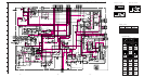
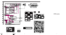
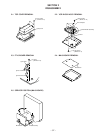
6-3. PRINTED WIRING BOARDS AND
SCHEMATIC DIAGRAMS
Note:
• All capacitors are in µF unless otherwise noted. pF: µµF
Capacitors without voltage indication are all 50V.
• All resistors are in ohms.
kΩ = 1000Ω, MΩ = 1000kΩ
• Indication of resistance, which does not have one for rating electrical
power, is as follows.
Pitch: 5 mm
Rating electrical power: 1/4W(CHIP:1/10W)
• : nonflammable resistor.
• : fusible resistor.
•
Å
: internal component.
• : panel designation and adjustment for repair.
• All variable and adjustable resistors have characteristic curve B, unless
otherwise noted.
• : earth-chassis.
• The components identified by
C
in this basic schematic diagram have been
carefully factory-selected for each set in order to satisfy regulations regarding
X-ray radiation.
Should replacement be required, replace only with the value originally used.
(
Refer to PM601,R614,C614,IC607 and R638 adjustment on Page 70 .
)
• When replacing the part in below table, be sure to perform the related
adjustment.
Adjustment
(
C
)
PM601,R614,C614,IC607,
R638 ............ A Board
• Readings are taken with a color-bar signal input.
• Readings are taken with a 10MΩ digital multimeter.
• Voltage variations may be noted due to normal production tolerances.
• All voltages are in V.
• Circled numbers are waveform reference.
• : B + line
• : B – line.
•
P
: signal path.
V
V
F
FF10
MA10
A
CV
Reference information
RESISTOR : RN METAL FILM
: RC SOLID
: FPRD NONFRAMMABLE CARBON
: FUSE NONFRAMMABLE FUSIBLE
: RW NONFRAMMABLE WIREWOUND
: RS NONFRAMMABLE METAL OXIDE
: RB NONFRAMMABLE CEMENT
: Å
ADJUSTMENT RESISTOR
COIL : LF-8L MICRO INDUCTOR
CAPACITOR : TA TANTALUM
: PS STYROL
: PP POLYPROPYLENE
: PT MYLAR
: MPS METALIZED POLYESTER
: MPP METALIZED POLYPROPYLENE
: ALB BIPOLAR
: ALT HIGH TEMPERATURE
: ALR HIGH RIPPLE
2
3
4
5
6
7
8
9
0
!¡
!™
1
Ver.1.6
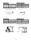
Transistor
Transistor
(Chip semiconductors that are not actually used are included.)
Diode
Diode
Diode
Diode
Diode
Diode
Diode
Diode
Diode
Diode
Anode
Anode
(NC)
(NC)
Cathode
Anode
Cathode
Common
Cathode
Cathode
Common
Cathode
Cathode
Common
Common
Common
Common
Cathode
Anode
Base
Emitter
Collector
Base
Emitter
Collector
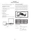
Device Printed symbol Terminal name
Circuit
Terminal name of semiconductors in silk screen
printed circuit ( )
Anode
Anode
Anode Cathode
Anode Anode
Cathode
Cathode
Anode
Anode
Cathode
Anode
Anode
*
A
[
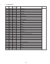
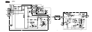
TUNER, Y/C/J, HV DEFLECTION, POWER SUPPLY
]
A BOARD
D305 D-2
D307 D-2
D308 E-3
D501 C-1
D502 D-1
D503 C-1
D506 C-2
D507 C-1
D601 B-6
D602 B-5
D603 B-5
D604 B-6
D605 D-6
D606 C-6
D607 C-7
D608 D-3
D609 D-5
D610 D-5
D611 B-5
D612 D-4
D613 C-5
D614 D-4
D615 A-5
D616 C-5
D617 C-6
D618 C-6
D619 C-6
D620 C-6
D621 C-5
D622 C-5
D623 D-4
D624 E-4
D625 D-6
D626 E-4
D627 D-4
D628 C-5
D629 E-4
D630 B-5
D631 C-5
D632 D-4
D633 D-2
D634 D-4
D801 C-1
D802 A-1
D803 C-2
D804 A-3
D805 D-1
D806 C-2
D807 A-3
D810 A-2
D811 A-3
IC
IC101 C-4
IC103 A-4
IC301 E-2
IC501 C-1
IC601 E-7
IC602 C-4
IC603 D-7
IC604 D-4
IC605 D-6
IC606 C-6
IC607 D-4
IC608 D-2
IC801 E-1
TRANSISTOR
*
Q101 B-4 1
Q102 A-4 1
Q103 A-4 1
Q301 D-1 1
Q302 D-2 1
Q303 D-2 1
Q304 D-2 1
Q305 E-3 1
Q501 D-2 1
Q502 D-2 1
Q503 D-1 1
Q601 D-5 1
Q602 E-4 1
Q604 E-4 1
Q605 C-5 -
Q606 D-3 1
Q607 C-5 1
Q608 D-4 1
Q609 C-7 1
Q610 D-4 1
Q801 C-2 -
Q802 B-2 -
Q803 B-3 -
DIODE
*
D101 A-4
D102 A-5
D103 C-4
D301 E-2
D302 E-2
D304 E-2
NOTE:
The circuit indicated as left contains high voltage of over
600 Vp-p. Care must be paid to prevent an electric shock in
inspection or repairing.
1234567
A
B
C
D
E
– A BOARD –