


3-27
PFM-42B1, PFM-42B1E
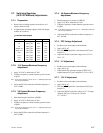
3-7. Switching Regulator
(APS-132 M Board) Adjustments
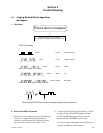
3-7-1. Preparation
1. Remove the switching regulator from the set, and
adjust it under no load.
2. If adjusting the switching regulator with each output
loaded, set as follows.
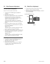
..
..
. Load on each output
3-7-2. 13 V System Minimum Frequency
Adjustment
1. Apply 18 V DC to both ends of C169.
2. Connect a frequency counter between gate and source
of Q153.
Note : As the input of frequency counter, use 10 : 1 oscilloscope probes and
raise the input impedance.
3. Adjust the RV150 so that the oscillation frequency is
93 ± 0.5 kHz.
3-7-3. VS System Minimum Frequency
Adjustment
1. Short between pin-3 and pin-4 of PH501.
2. Apply 18 V DC to both ends of C169.
3. Connect a frequency counter between gate and source
of Q503.
Note : As the input of frequency counter, use 10 : 1 oscilloscope probes and
raise the input impedance.
4. Adjust the RV500 so that the oscillation frequency is
49 ± 0.5 kHz.
3-7-4. VA System Minimum Frequency
Adjustment
1. Short between pin-3 and pin-4 of PH701.
2. Apply 18 V DC to both ends of C169.
3. Connect a frequency counter between gate and source
of Q703.
Note : As the input of frequency counter, use 10 : 1 oscilloscope probes and
raise the input impedance.
4. Adjust the RV700 so that the oscillation frequency is
65 ± 0.5 kHz.
3-7-5. PFC Voltage Adjustment
1. Set the load on each output to the minimum.
2. Apply 100 V AC.
3. Turn the STBY signal ON. (short between CN7 pin-1
and pin-2).
4. Adjust the RV300 so that the voltage across C115 is
385 ± 2 V.
3-7-6. 5 V Adjustment
1. Set the load on each output to the minimum.
2. Apply 100 V AC.
3. Adjust the RV201 so that the voltage of STBY +5 V
output (between CN7 pin-2 and pin-6) is 5.12 ± 0.03 V.
3-7-7. 13.5 V Adjustment
1. Set the load on each output to the minimum.
2. Apply 100 V AC.
3. Turn the STBY signal ON. (short between CN7 pin-1
and pin-2).
4. Adjust the RV250 so that the voltage of 13.5 V output
(between CN7 pin-12 and pin-11) satisfies
13.7 ± 0.05 V.
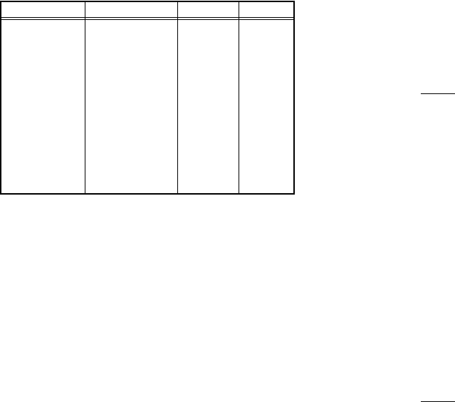
Output Pin No. MIN MAX
VCC CN4 1 pin 1.0 A 5.0 A
VS CN5 2 pin 0.5 A 1.7 A
VA CN5 5 pin 0.5 A 1.5 A
AUDIO +B CN6 3 pin 0.05 A 1.0 A
STBY +5 V CN7 2 pin 0.2 A 0.3 A
5VD CN7 5 pin 1.2 A 1.8 A
6.2 V CN7 8 pin 0.6 A 1.0 A
13.5 V CN7 != pin 0.5 A 1.0 A
13 V CN7 !] pin 0.4 A 1.0 A