


13-2
Instrument Block Diagrams
Introduction
Introduction
This chapter contains the block diagrams for the HP/Agilent 8922A/B/E/F/G/H/M/S.
Additional information for troubleshooting to the block diagram level can be found in the
following chapters.
Chapter 4, Using the Service Kit, explains how to use the HP/Agilent 83210A Service Kit
to extend the modules and make signal measurements.
Chapter 5, Troubleshooting the Controller/Display, gives procedures for troubleshooting
display problems or problems with the HP/Agilent 8922 Controllers.
Chapter 6, Troubleshooting the Power Supply, contains information about the power
supply and regulator circuits as well as test points and power distribution.
Chapter 12, Module I/O Specs, contains detailed descriptions of the input and output
signal characteristics for most RF and Audio modules.
Chapter 14, Block Diagram Theory, has a detailed technical discussion of the function of
each assembly in the block diagrams.
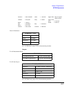
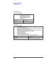
Reading the Pin Numbers
The signal names and pin numbers are shown on the diagrams, the pin numbers are
numbered according to the plug number found on the module, the jack number found on
the mother board, and the pin number.
For example: P2/J23(14)
P2 indicates that the signal is found on the module at Plug 2.
J23 indicates the signal is found on the mother board on Jack 23.
(14) indicates that pin number 14 (On plug 2 and Jack 23) carries the signal.
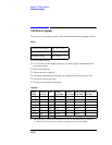
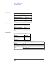
Block Diagram 1
Block Diagram 1 contains the RF and Audio Analyzer circuits in the HP/Agilent 8922.
These are the primary circuits used to make measurements. The Spectrum Analyzer is an
option in the HP/Agilent 8922F/H/M/S. The 14 dB input attenuator is replaced with an 8
dB attenuator in the HP/Agilent 8922F/H/M/S.
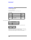
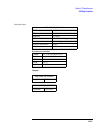
Block Diagram 2
Block Diagram 2 contains the RF and Audio Generator circuits. This block diagram
contains the generator hardware that is common to all three models of HP/Agilent 8922.