


37
3.2 Clock Supply
Note:
To supply the main clock signal from the user system, add an oscillation circuit to the user
system and have the main clock supplied via a CMOS buffer.
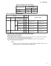
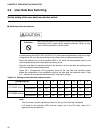
Table 3.2-1 Settings for main clock selection
Main clock source
FC SEL setting
12
Clock area OFF OFF
User system ON ON
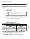
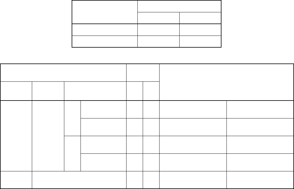
Table 3.2-2 Settings for subclock selection
Subclock
FC SEL
setting
SUB XTAL setting
Availability
Source
(*1)
Pin corresponding to
the evaluation MCU
(*2)
34
Available Clock area PGA
299
X1A: Pin No. 267
X0A: Pin No. 217
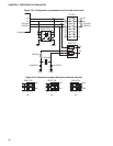
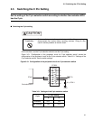
OFF OFF X1A:B connected to X1A:C
(a) in Figure 3.2-3
X0A:B connected to X0A:C
(a) in Figure 3.2-3
X1A: Pin No. 217
X0A: Pin No. 267
OFF OFF X1A:B connected to X0A:B
(b) in Figure 3.2-3
X1A:C connected to X0A:C
(b) in Figure 3.2-3
PGA
256
X1A: Pin No. 51
X0A: Pin No. 176
OFF OFF X1A:B connected to X1A:C
(a) in Figure 3.2-3
X0A:B connected to X0A:C
(a) in Figure 3.2-3
X1A: Pin No. 176
X0A: Pin No. 51
OFF OFF X1A:B connected to X0A:B
(b) in Figure 3.2-3
X1A:C connected to X0A:C
(b) in Figure 3.2-3
Not
available
-
ON ON X1A:A connected to X1A:B
(c) in Figure 3.2-3
X0A:A connected to X0A:B
(c) in Figure 3.2-3
*1: Clock oscillation with a crystal unit mounted in the user system is not supported.
*2: In the table, PGA299 and PGA256 indicate different adapter boards, which are:
PGA299: Adapter board for the PGA-299P
PGA256: Adapter board for the PGA-256P
The correspondence between subclock signals (X0A and X1A) and pin numbers on the evaluation MCU depends on the
evaluation MCU used. Check the correspondence before making settings.
For more information on the correspondence between subclock signals and pin numbers on the evaluation MCU,
contact the Fujitsu Sales Dept. or Support Dept.