


Service Modes, Error Codes, and Fault Finding
EN 19Q549.2E LA 5.
2009-May-08
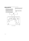
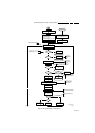
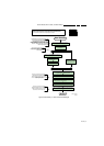
Figure 5-4 “Off” to “Semi Stand-by” flowchart (part 1)
No
EJTAG probe
connected ?
No
Yes
Release AVC system reset
Feed warm boot script
To I_17660_125b.eps To I_17660_125b.eps
Cold boot?
Yes
No
Set I²C slave address
of Standby µP to (A0h)
An EJTAG probe (e.g. WindPower ICE probe) can
be connected for Linux Kernel debugging
purposes.
This will allow access to NVM and
NAND FLASH and can not be done
earlier because the FLASH needs to
be in Write Protect as long as the
supplies are not available.
Detect EJTAG debug probe
(pulling pin of the probe interface to
ground by inserting EJTAG probe)
Release AVC system reset
Feed cold boot script
Release AVC system reset
Feed initializing boot script
disable alive mechanism
Initialise I/O pins of the st-by µP:
- Switch reset-AVC LOW (reset state)
- Switch WP-NandFlash LOW (protected)
- Switch reset-system LOW (reset state)
- Switch reset-5100 LOW (reset state)
- Switch reset-Ethernet LOW (reset state)
- Switch reset-ST7100 LOW (reset state)
- keep reset-NVM high, Audio-reset and Audio-Mute-Up HIGH
Off
Standby Supply starts running.
All standby supply voltages become available .
st-by µP resets
Stand by or
Protection
Mains is applied
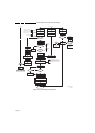
-Switch Audio-Reset high.
It is low in the standby mode if the standby
mode lasted longer than 10s.
start keyboard scanning, RC detection. Wake up reasons are
off.
If the protection state was left by short circuiting the
SDM pins, detection of a protection condition during
startup will stall the startup. Protection conditions in a
playing set will be ignored. The protection mode will
not be entered.
Switch LOW the RESET-NVM line to allow access to NVM. (Add a
2ms delay before trying to address the NVM to allow correct NVM
initialization, this is not issue in this setup , the delay is automatically
covered by the architectural setup)
Release Reset-PNX5100.
PNX5100 will start booting.
Wait 10ms (minimum) to allow the bootscript
of the PNX5100 to configure the PCI arbiter
Before PNX8541 boots, the PNX5100 should have
set its PCI arbiter (bootscript command). To allow
this, approx. 1ms is needed. This 1ms is extended
to 10ms to also give some relaxation to the supplies.
Switch HIGH the WP-NandFlash to
allow access to NAND Flash
+12V, +/-12Vs, AL and Bolt-on power
is switched on, followed by the +1V2 DCDC converter
Enable the supply fault detection
algorithm
No
Yes
Detect-1 I/O line
High?
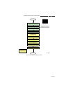
Switch ON Platform and display supply by switching
LOW the Standby line.
This enables the +3V3 and
+5V converter. As a result,
also +5V-tuner, +2V5, +1V8-
PNX8541 and +1V8-PNX5100
become available.
yes
Enable the DCDC converter for +3V3 and
+5V. (ENABLE-3V3)
Voltage output error:
Layer1: 2
Layer2: 18
Important remark; the appearance of the +12V
will start the +1V2 DCDC converter automatically
No
Yes
Supply-fault I/O
High?
The supply-fault line is a
combination of the DCDC
converters and the audio
protection line.
1V2 DCDC or class D error:
Layer1: 2
Layer2: 19
Enter protection
No
Detect2 high received
within 1 second?
Power-OK error:
Layer1: 3
Layer2: 16
Enter protection
Yes
No
Supply-fault I/O
High?
3V3 / 5V DCDC or class D error:
Layer1: 2
Layer2: 11
Enter protection
Wait 50ms
Enter protection
Delay of 50ms needed because of the latency of the detect-1 circuit.
This delay is also needed for the PNX5100. The reset of the
PNX5100 should only be released 10ms after powering the IC.
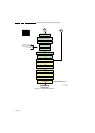
Detect2 should be polled on the standard 40ms
interval and startup should be continued when
detect2 becomes high.
Yes
No
Detect-2 I/O line
High?
Disable 3V3, switch standby
line high and wait 4 seconds
Added to make the system more robust to
power dips during startup. At this point the
regular supply fault detection algorithm which
normally detects power dips is not up and
running yet.
I_17660_125a.eps
140308