


List of Figures (Conclude)
Figure Title Page
Number Number
12-1 Counter A Block Diagram...........................................................................................12-2
12-2 Counter A Control Register (CACON) .......................................................................12-3
12-3 Counter A Registers................................................................................................... 12-3
12-4 Counter A Output Flip-Flop Waveforms in Repeat Mode ..........................................12-5
13-1 Simplified Timer 2 Function Diagram: Capture Mode................................................13-2
13-2 Simplified Timer 2 Function Diagram: Interval Timer Mode.......................................13-3
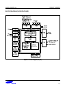
13-3 Timer 2 Block Diagram...............................................................................................13-4
13-4 Timer 2 Control Register (T2CON) ............................................................................13-5
13-5 Timer 2 Registers (T2CNTH, T2CNTL, T2DATAH, T2DATAL).................................13-6
14-1 Program Memory Address Space..............................................................................14-2
14-2 Smart Option ..............................................................................................................14-3
14-3 Flash Memory Control Register (FMCON).................................................................14-5
14-4 Flash Memory User Programming Enable Register (FMUSR)..................................14-5
14-5 Flash Memory Sector Address Register (FMSECH) .................................................14-6
14-6 Flash Memory Sector Address Register (FMSECL) .................................................. 14-6
14-7 Sector Configurations in User Program Mode ...........................................................14-7
14-8 Sector Erase Flowchart in User Program Mode ........................................................14-8
14-9 Byte Program Flowchart in a User Program Mode ....................................................14-12
14-10 Program Flowchart in a User Program Mode ............................................................14-13
15-1 Low Voltage Detect (LVD) Block Diagram.................................................................15-3
15-2 Low Voltage Detect Control Register (LVDCON) ......................................................15-4
15-3 Low Voltage Detect Flag Selection Register (LVDSEL) ............................................15-4
16-1 Stop Mode Release Timing When Initiated by an External Interrupt.........................16-6
16-2 Stop Mode Release Timing When Initiated by a LVD................................................16-7
16-3 Input Timing for External Interrupts (Port 0 and Port 2).............................................16-8
16-4 Operating Voltage Range of S3F80P5.......................................................................16-11
17-1 24-Pin SOP Package Mechanical Data .....................................................................17-1
17-2 24-Pin SDIP Package Mechanical Data ....................................................................17-2
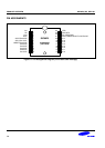
18-1 Pin Assignment Diagram (24-Pin SOP/SDIP Package) ............................................18-2
19-1 Development System Configuration...........................................................................19-2
19-2 TB80PB Target Board Configuration .........................................................................19-3
19-3 50-Pin Connector Pin Assignment for User System ..................................................19-6
19-4 TB80PB Probe Adapter Cable ...................................................................................19-6
S3F80P5_UM_REV1.00 MICROCONTROLLER xiii