


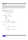
S3F80P5_UM_ REV1.00 RESET
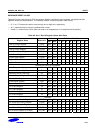
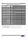
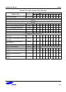
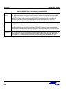
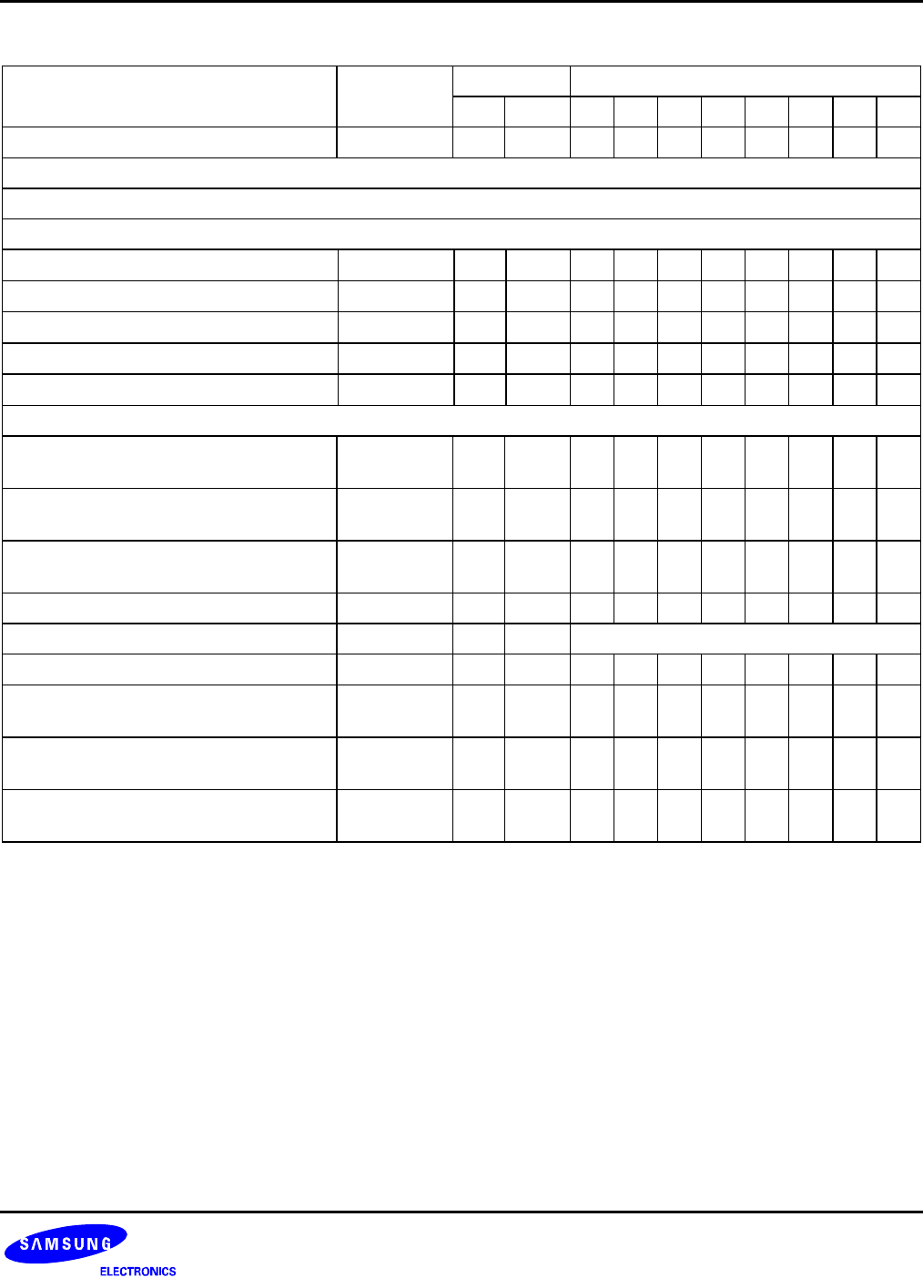
Table 8-3. Set 1, Bank 1 Register Values After Reset
Address Bit Values After Reset
Register Name Mnemonic
Dec Hex 7 6 5 4 3 2 1 0
LVD Control Register LVDCON 224 E0H – – – – – – – 0
Reserved
Reserved
Reserved
Timer 2 Counter Register (High Byte) T2CNTH 228 E4H 0 0 0 0 0 0 0 0
Timer 2 Counter Register (Low Byte) T2CNTL 229 E5H 0 0 0 0 0 0 0 0
Timer 2 Data Register (High Byte) T2DATAH 230 E6H 1 1 1 1 1 1 1 1
Timer 2 Data Register (Low Byte) T2DATAL 231 E7H 1 1 1 1 1 1 1 1
Timer 2 Control Register T2CON 232 E8H 0 0 0 0 0 0 0 0
Not mapped in address E9H to EB
Flash Memory Sector Address Register
(High Byte)
FMSECH 236 ECH 0 0 0 0 0 0 0 0
Flash Memory Sector Address Register
(Low byte)
FMSECL 237 EDH 0 0 0 0 0 0 0 0
Flash Memory User Programming
Enable Register
FMUSR 238 EEH 0 0 0 0 0 0 0 0
Flash Memory Control Register FMCON 239 EFH 0 0 0 0 – – – 0
Reset Indicating Register RESETID 240 F0H Refer to the section 4.control registers
LVD Flag Level Selection Register LVDSEL 243 F1H 0 0 – – – – – –
PORT1 Output Mode Pull-up Enable
Register
P1OUTPU 244 F2H 0 0 0 0 0 0 0 0
PORT2 Output Mode Selection
Register
P2OUTMD 245 F3H 0 0 0 0 0 0 0 0
PORT3 Output Mode Pull-up Enable
Register
P3OUTPU 246 F4H – – 0 0 – – 0 0
8-17