


RESET S3F80P5_UM_ REV1.00
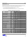
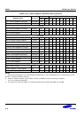
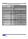
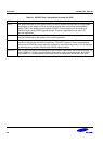
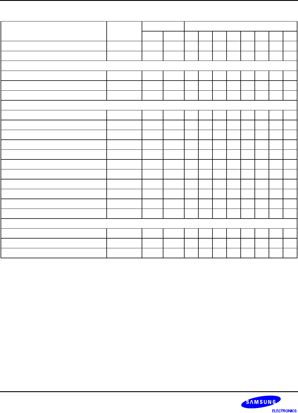
Table 8-2. Set 1, Bank 0 Register Values After Reset (Continued)
Address Bit Values After Reset
Register Name Mnemonic
DecHex7654 3 2 10
Port 1 Control Register (High Byte) P1CONH 234 EAH 1 1 1 1 1 1 1 1
Port 1 Control Register (Low Byte) P1CONL 235 EBH 0 0 0 0 0 0 0 0
Reserved
Port 2 Control Register (Low Byte) P2CONL 237 EDH 0 0 0 0 0 0 0 0
Port 2 Pull-up Enable Register P2PUR 238 EEH 0000 0 0 00
Port 3 Control Register P3CON 239 EFH 0000 0 0 00
Reserved
Port 0 Interrupt Enable Register P0INT 241 F1H 0000 0 0 00
Port 0 Interrupt Pending Register P0PND 242 F2H 0000 0 0 00
Counter A Control Register CACON 243 F3H 0000 0 0 00
Counter A Data Register (High Byte) CADATAH 244 F4H 1111 1 1 11
Counter A Data Register (Low Byte) CADATAL 245 F5H 1111 1 1 11
Timer 1 Counter Register (High Byte) T1CNTH 246 F6H 0000 0 0 00
Timer 1 Counter Register (Low Byte) T1CNTL 247 F7H 0000 0 0 00
Timer 1 Data Register (High Byte) T1DATAH 248 F8H 1111 1 1 11
Timer 1 Data Register (Low Byte) T1DATAL 249 F9H 1111 1 1 11
Timer 1 Control Register T1CON 250 FAH 0000 0 0 00
STOP Control Register STOPCON 251 FBH 0000 0 0 00
Locations FCH is not mapped. ( For factory test )
Basic Timer Counter BTCNT 253 FDH 0000 0 0 00
External Memory Timing Register EMT 254 FEH 0111 1 1 0–
Interrupt Priority Register IPR 255 FFH x x x x x x x x
NOTES:
1. Although the SYM register is not used, SYM.5 should always be “0”. If you accidentally write a 1 to this bit during normal
operation, a system malfunction may occur.
2. Except for T0CNTH, T0CNTL, IRQ, T1CNTH, T1CNTL, and BTCNT, which are read-only, all registers
in set 1 are read/write addressable.
3. You cannot use a read-only register as a destination field for the instructions OR, AND, LD, and LDB.
8-16