


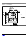
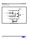
S3F80P5_UM_ REV1.00 PRODUCT OVERVIEW
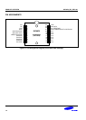
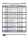
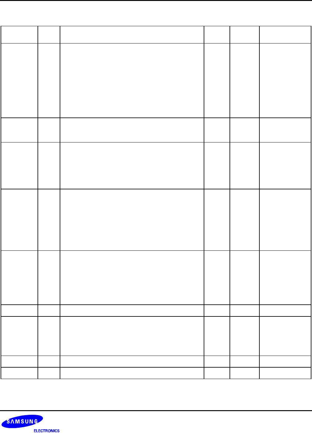
Table 1-1. Pin Descriptions of 24-SOP/SDIP
Pin
Names
Pin
Type
Pin Description
Circuit
Type
28 Pin
No.
Shared
Functions
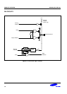
P0.0−P0.7
I/O I/O port
with bit-programmable pins. Configurable
to input or push-pull output mode. Pull-up resistors
are assignable by software. Pins can be assigned
individually as external interrupt inputs with noise
filters, interrupt enable/ disable, and interrupt
pending control. SED&R (note) circuit built in P0
for STOP releasing.
In the tool mode, P0.0 and P0.1 are assigned as
serial MTP interface pins; SDAT and SCLK
1 5-12 Ext. INT
(INT0−INT3)
(INT4)
(SDAT)
(SCLK)
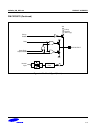
P1.0−P1.7
I/O I/O port with bit-programmable pins. Configurable
to input mode or output mode. Pin circuits are
either push-pull or n-channel open-drain type.
2
13-20
−
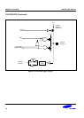
P2.0
I/O I/O port with bit-programmable pin. Configurable to
input mode, push-pull output mode, or n-channel
open-drain output mode. Pull-up resistor can be
assigned by software. Pin can be assigned as
external interrupt input with noise filter, interrupt
enable/disable, and interrupt pending control.
3
23 Ext. INT
(INT5)
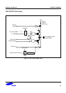
P3.0
I/O I/O port with bit-programmable pin. Configurable to
input mode, push-pull output mode, or n-channel
open-drain output mode. Input mode with a pull-up
resistor can be assigned by software.
This port 3 pin has high current drive capability.
Also P3.0 can be assigned individually as an
output pin for T0PWM or input pin for
T0CAP/T1CAP/T2CAP.
4 26 T0PWM/T0CAP/
T1CAP/T2CAP
P3.1
I/O I/O port with bit-programmable pin. Configurable to
input mode, push-pull output mode, or n-channel
open-drain output mode. Input mode with a pull-up
resistor can be assigned by software.
This port 3 pin has high current drive capability.
Also P3.1 can be assigned individually as an
output pin for REM or input pin for T0CK.
5 27 REM/T0CK
X
OUT,
X
IN
– System clock input and output pins – 2,3
−
TEST
I Test signal input pin
If on board programming is needed, It is
recommended that add a 0.1uF capacitor between
TEST pin and VSS for better noise immunity;
otherwise, connect TEST pin to VSS directly.
−
4
−
V
DD
−
Power supply input pin
−
28
−
V
SS
−
Ground pin
−
1
−
1-5