


S3F80P5_UM_ REV1.00 ELECTRICAL DATA
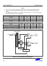
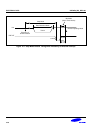
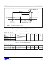
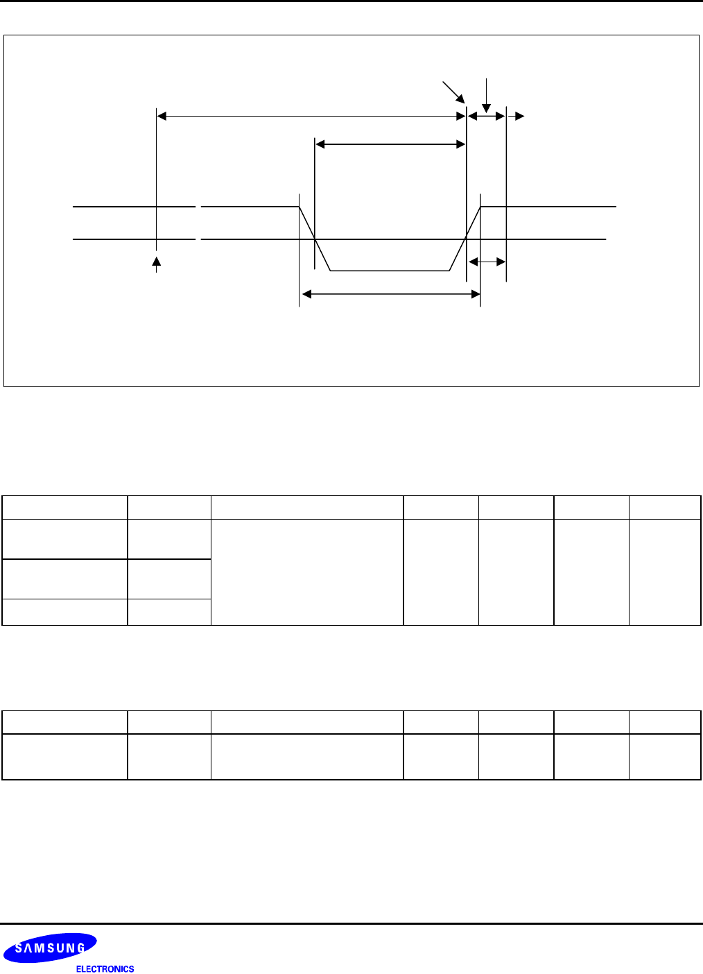
Normal Operating Mode
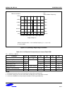
Stop Mode
Oscillation Stabilization Time
Reset
Occur
Execution of
STOP Instrction
V
DD
NOTE:
t
WAIT
is the same as 4096 x 16 x 1/f
OSC
.
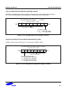
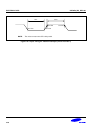
V
LVD
~
~
Data Retention Time
V
DDDR
Back-up Mode
t
WAIT
~
~
Figure 16-2. Stop Mode Release Timing When Initiated by a LVD
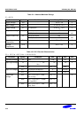
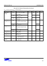
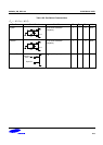
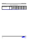
Table 16-6. Input/Output Capacitance
(T
A
= -25 °C to + 85 °C)
Parameter Symbol Conditions Min Typ Max Unit
Input
Capacitance
C
IN
− −
10 pF
Output
Capacitance
C
OUT
I/O Capacitance
C
IO
f = 1 MHz
V
DD
= 0 V, unmeasured pins
are connected to V
SS
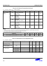
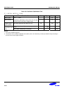
Table 16-7. A.C. Electrical Characteristics
(T
A
= -25 °C to + 85 °C)
Parameter Symbol Conditions Min Typ Max Unit
Interrupt Input
High, Low Width
t
INTH
,
t
INTL
P0.0−P0.7, P2.0
V
DD
= 3.6 V
200 300
−
ns
16-7