


RESET S3F80P5_UM_ REV1.00
RESET MECHANISM
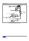
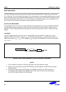
The interlocking work of reset pin and LVD circuit supplies two operating modes: back-up mode input, and system
reset input. Back-up mode input automatically creates a chip stop state when the voltage at V
DD
is lower than
V
LVD
. When the LVD circuit detects rising edge of V
DD
on the point V
LVD
, the reset pulse generator makes a reset
pulse, and system reset occurs. When the operating mode is in STOP mode, the LVD circuit is disabled to reduce
the current consumption under 5uA (at V
DD
= 3.6 V). Therefore, although the voltage at V
DD
is lower than V
LVD
,
the chip doesn’t go into back-up mode when the operating state is in stop mode.
WATCH DOG TIMER RESET
The watchdog timer that can recover to normal operation from abnormal function is built in S3F80P5. Watchdog
timer generates a system reset signal, if Basic Timer Counter (BTCNT) isn’t cleared within a specific time by
program. For more understanding of the watchdog timer function, please see the chapter 10, Basic Timer and
Timer0.
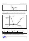
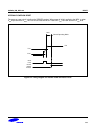
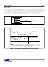
LVD RESET
The Low Voltage Detect Circuit (LVD) is built on the S3F80P5 product to generate a system reset. LVD is
disabled in stop mode. When the voltage at V
DD
is falling down and passing V
LVD
, the chip goes into back-up
mode at the moment “V
DD
= V
LVD
”. As the voltage at V
DD
is rising up, the reset pulse is occurred at the moment
“V
DD
≥ V
LVD
“.
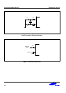
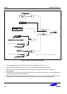
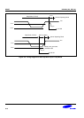
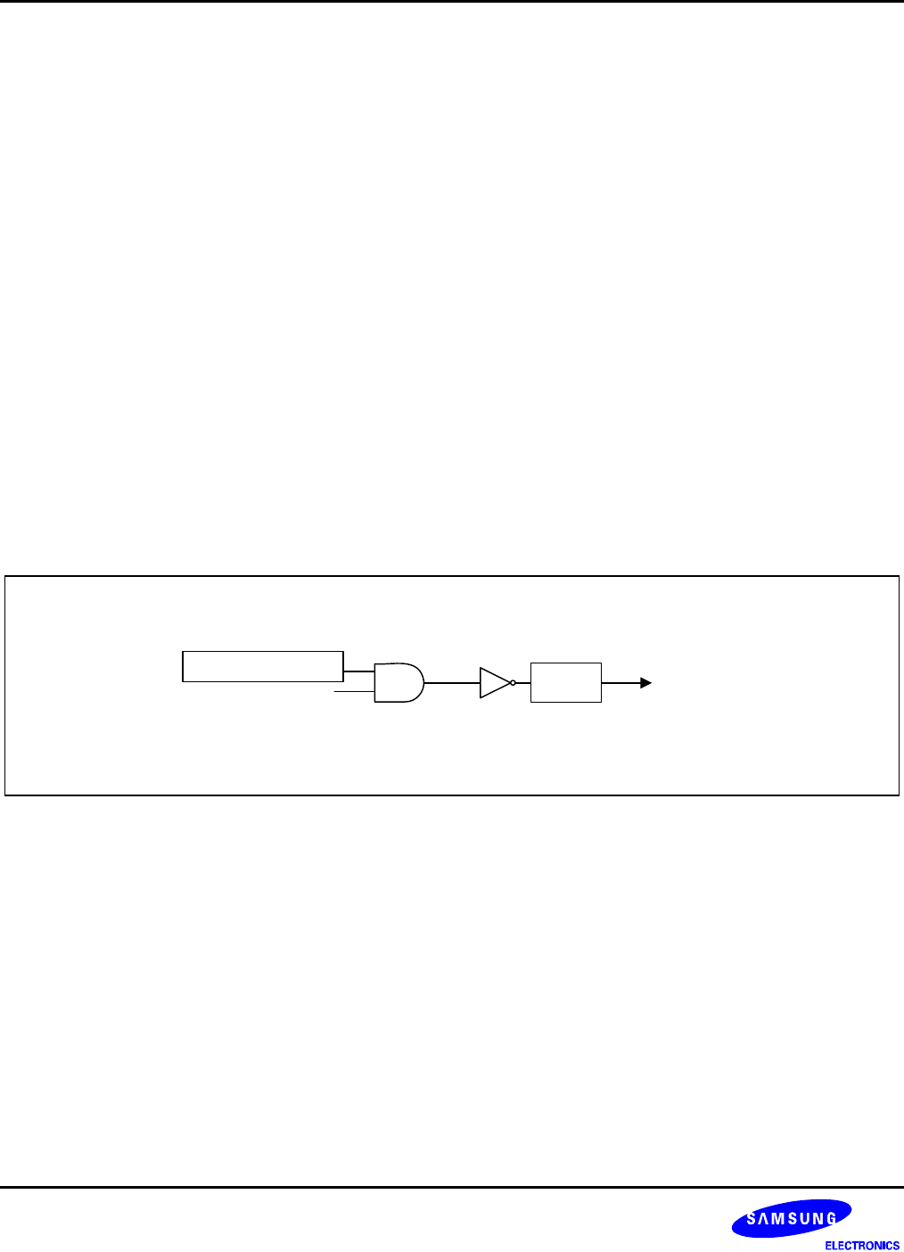
STOP Instruction
ResetLVD
STOPCON
(note 2)
(note 3)
Figure 8-3. RESET Block Diagram by LVD for the S3F80P5 in Stop Mode
NOTES
1. LVD is disabled in stop mode. LVD always operates in any other operation modes.
2. CPU can enter stop mode by setting STOPCON (Stop Control Register) into 0A5H before execution
STOP instruction.
3. This signal is output relating to STOP mode. If STOPCON has 0A5H, and STOP instruction is
executed, that output signal makes S3F80P5 enter STOP mode. So that is one of two statuses;
one is STOP mode, the other is not STOP mode.
8-4