176 Advanced Programming with the VT1529B Chapter 5
Field Wiring for dc
Voltage
Measurements
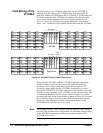
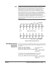
There are separate input pins on the RJ-45 connector for the high-level and
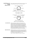
low-level DCV signals. See Figure 5-8 for the connector pin-out.
Low-Level Inputs The low-level input pins are limited to signals less than ±0.5 V dc.
These inputs can be balanced with respect to chassis ground or can be
single-ended. There are three optional low-pass filters that can be used
on the low-level inputs, with cut-off frequencies of 2, 10, and 100 Hz.
These filters are selected by the INPut:FILTer[:LPASS]:FREQuency
command. After the filter, the low-level inputs go through an amplifier to
give higher noise immunity before being sent to the VT1422A. When the
VT1422A measures the amplified low-level signal, it internally
compensates for the amplification so that the value sent to algorithms, the
CVT and the FIFO is the actual voltage at the low-level input pins.
High-Level Inputs The high-level input pins can accept signals up to 10 V dc. These inputs
should be balanced with respect to chassis. An unbalanced signal will not
settle quickly if a long cable is placed between the VT1422A and the
VT1529A/B, which can cause measurement errors both on the unbalanced
input as well as on the next few channels in the scan list.
There is no filtering or amplification in the high-level input path.
Figure 5-8. Pin-out for DCV Measurements
Shield Gnd
High-Level DCV
Shield Gnd
Pinout for Lower Connector Row
Low-Level DCV Sense
Excitation
Low-Level DCV Sense
-
Shield Gnd
Pinout for Upper Connector Row
Shield Gnd
321 45678
6
5
4
2
1
3
8
7
Low-Level DCV SenseLow-Level DCV Sense
Sense
+
-
+
+
-
-
-
+
+
-
+
High-Level DCV
Sense
Excitation
High-Level: signals >= ±0.5 VDC
Low-Level: signals <= ±0.5 VDC


