54 Field Wiring Chapter 2
Adding Components to the Terminal Module
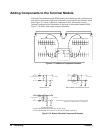
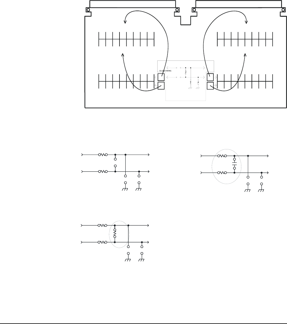
The back of the terminal module PCB (printed circuit board) provides surface mount
pads which can be used to add serial and parallel components to any channel's signal
path. Figure 2-17 shows additional component locator information (see the
schematic and pad layout information on the back of the terminal module PCB).
Figure 2-18 shows some usage example schematics.
Upper layout also applies here
Upper layout also applies here
Lower layout also applies here Lower layout also applies here
SCHEMATIC OF MODIFIABLE PARTS
HI HI
LO
LO
TO VT1413C/VT1415A
SH
SL
COMP
LOCATOR
COMP
LOCATOR
Figure 2-17. Additional Component Location
TO VT1422A
LO
HI
TO USER WIRING
PHL
PH
PL
0 ohms
0 ohms
LO
HI
Default Circuit
SH
SL
PHL
LO
HI
TO VT1422A
SH
LO
HI
PH
PL
SL
10 kohms
10 kohms
Normal Mode Low-Pass Filter Circuit
TO USER WIRING
LO
HI
SH
0 ohms
SL
0 ohms
PHL
250 ohms
or
200 ohms
TO VT1422A
HI
LO
PH
PL
4-20 mA NOTE: input must not exceed common mode limits (usually
±16 volts unless attenuated with a VT1513A SCP)
4 to 20 mA Sense
5 V full scale with 250 ohm (must use 16 volt range)
4 V full scale with 200 ohm (can use 4 volt range for better resolution)
0.1 Fµ
Figure 2-18. Series & Parallel Component Examples


