


5-3
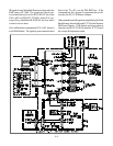
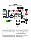
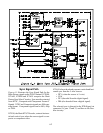
The Sub picture signals from IC2B00 are directed to
IC2G00, the Sub Decoder. Switch circuitry in IC2G00
selects Sub picture signals from IC2B00 or the AV-
SW(2), IC2K00.
As in previous chassis, the main and sub selected YPbPr
signal are direct to the PCB-SIGNAL.
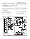
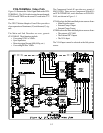
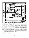
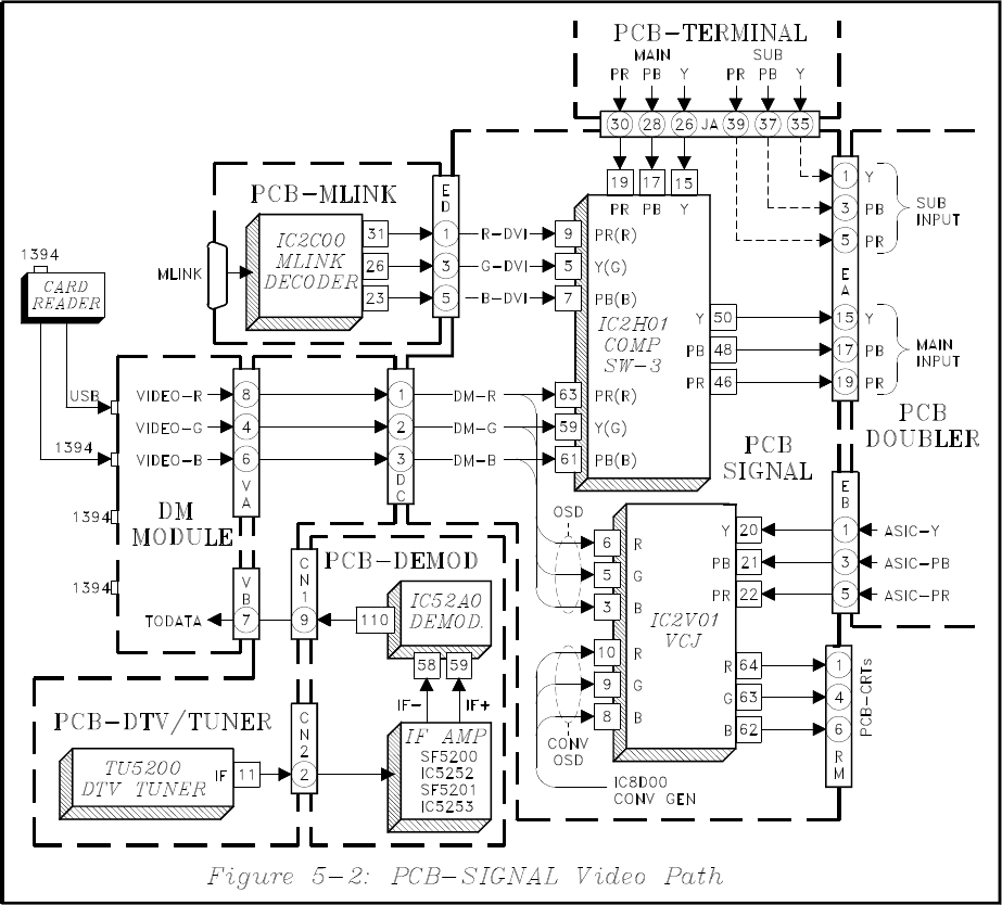
PCB-SIGNAL Video Path
Figure 5-2 shows the PCB-SIGNAL Video Signal Path.
Sub picture signals from PCB-TERMINAL are routed
directly to the Sub YPbPr inputs of PCB-DOUBLER.
The main picture signals from PCB-TERMINAL are
routed to COMP SW-3, IC2H01. IC2H01 selects the
main signal from the PCB-TERMINAL main outputs,
or the MLINK signal from the MLINK Decoder, or
the RGB signal from the DM Module. The output of
IC2H01 is applied to the Main Picture inputs to the
Doubler circuit.
Note that the OSD RGB signals from the DM Module
are also directed the VCJ, IC2V01.
On-Screen Display (OSD) signals are generated in the
DM Module, and when the signal source is not the DM,
OSD is inserted in the main picture in the VCJ. If the
source is from the DM, the DTV Tuner or 1394 inputs,
OSD insertion occurs in the DM module.
The diagram also shows that Convergence OSD sig-
nals are applied to the VCJ and inserted in the VCJ.