


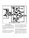
6-8
HV & HV Regulation
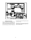
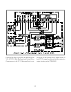
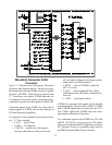
Figure 6-8 illustrates the HV and HV Regulation cir-
cuitry. Drive from the Horizontal Deflection Out-
put circuitry is applied the HD-IN input of IC5A00.
IC5A00 amplifies the signal which is output at pin
1, and through Q5A07 and Q5A09, is applied to the
gate of Q5A51.
The output of Q5A51 is the drive signal for the Fly-
back transformer, T5A51. In the Flyback, the sig-
nals are stepped up and rectified to generate the HV
and Focus voltages for the three CRTs.
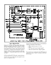
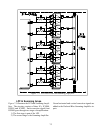
The amount of HV generated depends of the con-
duction time of Q5A51, the longer the conduction
time the more energy supplied to the Flyback, and
HV increases. HV is regulated by controlling the
duty cycle of the drive signal to Q5A31.
A sample of the HV, HV-DC-FB, is derived from an
internal resistive divider in the Flyback and is out-
put at pin 13. The HV sample is applied to the non-
inverting input of an OP-Amp in IC5A01. The HV
ADJ voltage in applied to the inverting input of a
second OP-Amp in IC5A01. The outputs of both
OP-Amps are combined and directed to pin 4 of
IC5A00.