


6-5
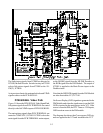
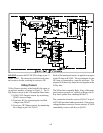
Vertical Deflection
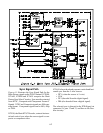
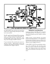
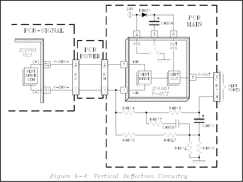
Figure 6-4 shows the Vertical Deflection circuitry.
The Vertical Deflection Generator in the VCJ out-
puts push-pull type of vertical deflection drive sig-
nal. +VDR at pin 53 and –VDR atz pin 52. Both
signals are applied to the Vertical Output IC, IC4B01.
The amplified output from IC4B01 is directed to the
vertical coils in the Deflection Yokes.
D4B01 and C4B04 make up the pump-up circuitry.
Feedback from the Deflection Yokes ground return
at pin 4 of DY, to pin 1 of IC4B01, provide linearity
and S correction.
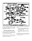
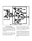
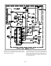
Horizontal Deflection
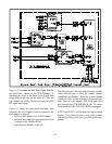
Figure 6-4 illustrates the Horizontal Deflection Drive
and Output circuitry. Horizontal drive signal from
the VCJ is amplified by Horizontal Drive circuitry
including transistors Q2V40, Q5A40, Q5A33,
Q5A39 and Q5A32.
The output from Q5A32 is directed to Q5A31, the
Horizontal Output transistor. The output from
Q5A31 takes three paths:
1) To the horizontal windings in the Deflection
Yokes
2) Through C5A34 and Q5A37 to the HV
Drive circuitry.
3) Through T5A31, providing the source for
the CRT filament supply.