Rev. 1.0, 07/01, page 365 of 372
DEC
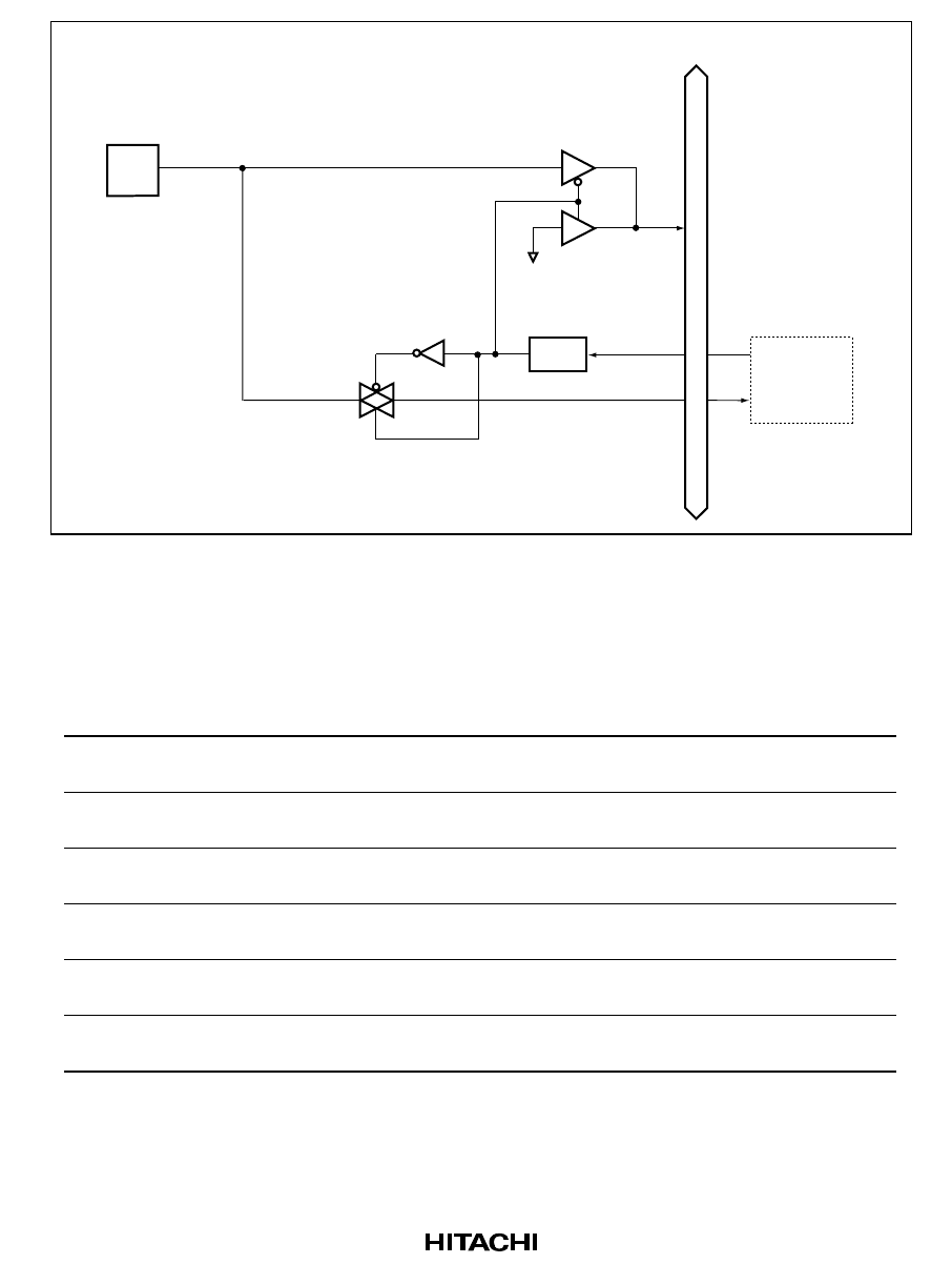
V
IN
CH3 to CH0
A/D converter
Internal data bus
Figure B.17 Port B Block Diagram (PB7 to PB0)
B.2 Port States in Each Operating State
Port Reset Sleep Subsleep Standby Subactive Active
P17 to P14,
P12 to P10
High
impedance
Retained Retained High
impedance*
Functioning Functioning
P22 to P20 High
impedance
Retained Retained High
impedance
Functioning Functioning
P57 to P50 High
impedance
Retained Retained High
impedance*
Functioning Functioning
P76 to P74 High
impedance
Retained Retained High
impedance
Functioning Functioning
P87 to P80 High
impedance
Retained Retained High
impedance
Functioning Functioning
PB7 to PB0 High
impedance
High
impedance
High
impedance
High
impedance
High
impedance
High
impedance
Note: *High level output when the pull-up MOS is in on state.


