


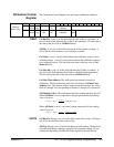
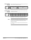

Card Control
Register
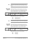
The Card Control Register allows for access to the A24 address space from
the A16 address space. It also provides access to the non-volatile memory.
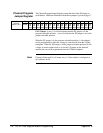
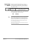
Address
Base + 1E
16
Bit 15 14 13 12 11 10 09 08 07 06 05 04 03 02 01 00
READ Unused VPPEN A24 Window
WRITE
VPPEN: Writing a one (1) to this field enables the non-volatile memory to be
altered. Writing a zero (0) disables updates or erasures of the non-volatile
memory. Non-volatile memory is located at base + 100
16
to base + 200
16
.
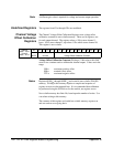
Note The VPPEN field enables or disables the programming voltage needed to
change the contents of the non-volatile memory. A physical jumper on the
main printed circuit board must also be moved to the CAL position before
the contents of the non-volatile memory can be altered.
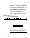
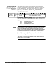
A24 Window: Writing a value to this field sets which 16 register-wide portion
of A24 registers can be accessed via A16 registers 20
16
to 3E
16
. The registers
mapped for each value are shown below and in Figure B-3 on page 116.
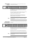
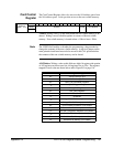
A24 Window Value A24 Registers Mapped
0
16
A16 00
16
through 1E
16
1
16
A16 20
16
through 3E
16
2
16
Main_DAC Immediate Registers
3
16
Main_DAC Triggered Registers
4
16
Offset_DAC Registers
5
16
Gain_DAC Registers
6
16
Undefined
7
16
Undefined
8
16
Voltage Offset Cal Memory (non-volatile)
9
16
Voltage Gain Cal Memory (non-volatile)
A
16
Current Offset Cal Memory (non-volatile)
B
16
Current Gain Cal Memory (non-volatile)
C
16
Cal and Configuration Registers (non-volatile)
D
16
Undefined Cal Memory (non-volatile)
E
16
Undefined Cal Memory (non-volatile)
F
16
Undefined Cal Memory (non-volatile)
Appendix B HP E1418A Register-Based Programming 137