


36
1. OUTLINE
A wide aspect conversion (hereafter called WAC) process (3/4
compression process in 4:3 mode and 1/2 compression process
on left screen in double window mode) is performed inside the
WAC unit (PB6348) in TW40F80.
Screen modes for TF40F80 contain THEATER WIDE1, THE-
ATER WIDE 2, THEATER WIDE3, FULL, NORMAL and
DOUBLE WINDOW modes. The video signal compression is
carried out only when either the NORMAL or DOUBLE WIN-
DOW mode is selected. In the modes other than the NORMAL
and DOUBLE WINDOW mode, the video signal input to WAC
unit is output without performing any process.
The screen in the DOUBLE WINDOW mode creates a single
screen by superimposing the left screen processed in the WAC
unit on the right screen processed in the DUAL unit.
On the left screen, the video signal sent is time-compressed to 1/
2 in horizontal direction to fit in the left half of the wide screen
with 16:9 aspect ratio. In this case, a black level of DC is at-
tached on the right half of the screen in this circuit. However,
this is superimposed on the right screen, so nothing is visible on
the screen.
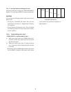
In the normal screen, the video signal is 3/4 time-compressed
and side panels in the black level are added on sides of the screen.
2. CIRCUIT OPERATION
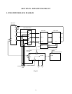
2-1. Configuration
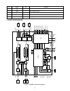
The WAC unit consists of a wide aspect conversion IC (QX01,
TC9097F, working as a central device), clock generation IC
(QX02, TA8667F), switch IC (QX03, TC4053BF), and periph-
eral circuits (LPF, AMP, emitter follower, etc.). The QX01
(TC9097F) contains an A/D converter, D/A converter, clamp cir-
cuit, VCO circuit, etc. and performs compression process, etc.
inside the IC for analog video signals entered according to con-
trols through IIC bus, thus providing the signal as an analog sig-
nal.
2-2. Operation
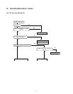
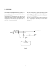
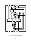
2-2-1. Signal Flow
Fig. 5-1 shows a block diagram of this circuit. A Y signal en-
tered through pin 6 of PX01 passes a low pass filter an a 6 dB
amplifier, and enters pin 3 of QX01. On the other hand, I and Q
signals enter through pin 4 and 5 of PX01,
and pass a low pass filter and amplifiers in the same way as the
Y signal, and enter pins 1 and 78 of QX01 respectively.
The Y , I and Q signals entered are clamped by built-in clamp
circuit, converted into digital signals by the built-in A/D con-
verter. Moreover, their read/write operations are rated up by twice
or 3/4 times to perform a compression process of 1/2 or 3/4
times inside the built-in line memory. And then, a black level
signal is added to the open area (right half, or both sides of
screen). Next, the signal is converted to an analog Y, I, and Q
signals by a built-in D/A converter and output from pins 17, 13,
and 9. Parameters of 1/2, 3/4 phase of the video signal, phase of
the side panel, etc. are controlled through I
2
C bus, control sig-
nals of which enters from pins 7 and 8 of PX01.
Thus processed signals are fed to a low pass filter to remove
high frequency noises generated in QX01 and then fed to the
QX03 switching IC. The compressed signal and a not compressed
signal entered from PX01 are directly fed to QX03, and switched
by a signal showing compression/not compression (NCS = out-
put from pin 61 of QX01 and fed to the receive unit through
pins 5, 6, and 7 of PX02.
2-2-2. Clock Generation
The system clock for QX01 is generated by QX02 according to
an H reference signal supplied from pin 3 of PX02 and fed to
QX01 through QX19 and QX40. (The frequency is adjusted to
28.7 ± 0.2 MHz with LX18).
The compressing operation is carried out by setting the write
clock to 1/2 or 3/4 times by the built-in VCO with the reading
clock fed to pin 47 of QX01.
2-2-3. Timing Pulse Generation
Moreover, the WAC unit generates following timing pulses.
(1) VPout
Reference signal entered through pin 2 of PX02 enters pin
3 of QX01, and outputs at pin 8 of PX02 after delayed by
an amount required. The vertical reference signal is out-
put in modes other than the normal and double window
and fed to the vertical circuit. Accordingly, the raster be-
comes an horizontal one when the unit is disconnected.
(2) HVBLK
This pulse is a timing pulse showing a black extension
mask period in the normal and double window modes. It
outputs at pin 1 of PX02 and enters pin 30 of Q501 in the
receive unit.
SECTION V: WAC CIRCUIT