40
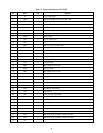
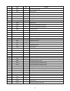
No.
38
39
40
41
42
43
44
45
46
47
48
49
50
51
52
53
54
55
56
57
58
59
60
61
62
63
64
65
66
67
68
69
70
71
72
73
74
75
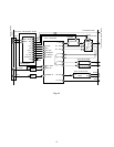
I/O
I
–
–
I
–
–
–
–
–
O
–
–
–
O
–
–
–
O
–
–
–
–
–
I
–
–
–
–
I
–
I
I
–
–
I
I
I
–
Name
HDF
GND
AVDD
VFL2
NC
AGND
CKSEL
VDD
WCK
RCK
HBL
NC
VBL
HRF
VMO
SPT
QSL
NC
ISL
VDP
ACP
SCL
SDA
NCS
SE42
NC
BCP
TD14
TD13
TD12
TD11
TD10
NC
GND
NC
NC
AVDD
VRA1
Function
Ext. H sync signal input
Digital ground
Analog power
Loop filter for VCO2
–
Analog ground
VDD
Digital power
Ext. clock input (memory write clock)
Ext. clock input (memory read clock)
H blanking signal
V blanking signal
H AFC reference signal
H AFC mask signal
Side panel timing signal
Q signal select pulse
–
I signal select pulse
V drive pulse
Later stage clamp pulse
I
2
C SCL signal input
I
2
C SDA signal input/output
Prefilter switch signal 1
Prefilter switch signal 2
–
Prestage clamp pulse output
Test input (normally connected to VSS)
Test input (normally connected to VSS)
Test input (normally connected to VSS)
Test input (normally connected to VSS)
Test input (normally connected to VSS)
–
Digital ground
Analog power
Reference voltage for AD1, AD2


