


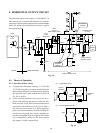
67
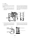
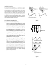
(4) To shorten the storage time and the falling time, a suf-
ficiently high reverse bias voltage must be applied to
allow a heavy reverse current to flow. This operation
also stabilizes operation of the horizontal output tran-
sistor.
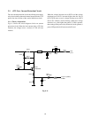
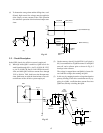
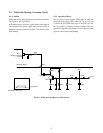
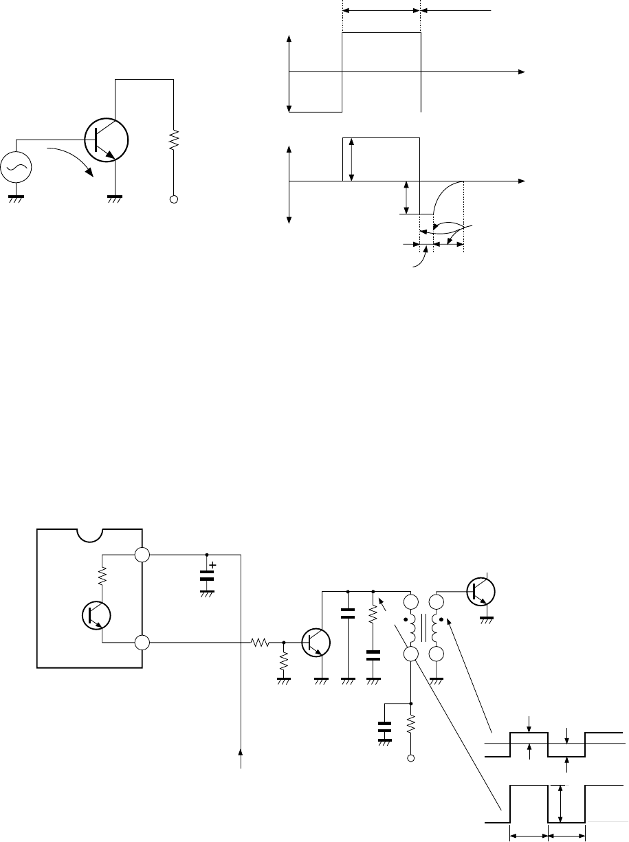
Fig. 9-3
Fig. 9-2
3-2. Circuit Description
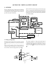
In the N5SS chassis, the off drive system is employed.
(1) When Q1 inside Q501 is turned on, Q402 base is for-
ward biased through 9V ® pin 22 of Q501 (H. VCC)
® pin 23 of Q501 (H. Out) ® R411/R410 resistor di-
vider, and then, Q402 collector current flows through
125V ® R416 ® T401. In this case, the H output tran-
sistor Q404 turns on with the base-emitter reverse bi-
ased because of the off drive system employed.
(2) On the contrary, when Q1 inside IC501 is off (pin 8 is
0V), base-emitter bias of Q402 becomes 0V and Q402
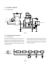
turns off, and a collector pulse as shown in Fig. 9-3
develops at the collector.
The voltage is stepped down and Q404 is forward bi-
ased with this voltage, thus turning on Q404.
(3) In this way, by stepping down the voltage developed at
primary winding of the drive transformer and by ap-
plying it to Q404, a sufficient base current flows into
Q404 base, thereby switching the Q404.
Q501
22
23
1
3
2
4
Q1
H. Vcc
C431
R410
R411
9V
Q402
H drive
transistor
C417
R415
T401
H drive
transistor
Q404
H output
transistor
V1
V2
0V
0V
VCP
Q402
OFF
Q402
ON
R416
C416
+125V
C413
+
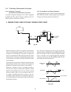
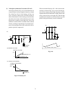
(a)
ib
V
+
0
-
+
0
-
On period OFF period
t Input waveform (b)
t Base current (c)
Forward
current
Reverse
current
Falling
time
Storage
time