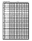
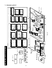
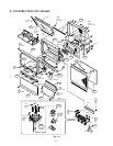
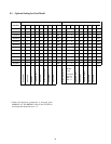
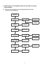
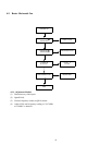
46
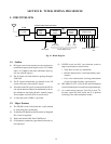
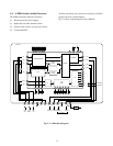
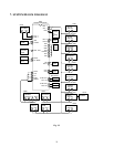
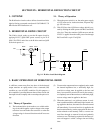
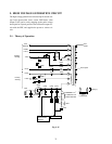
4. CIRCUIT OPERATION
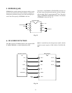
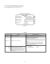
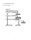
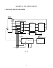
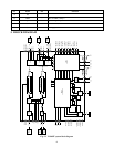
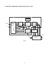
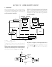
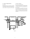
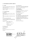
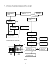
4-1. Video/Color/Deflection Process Section
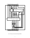
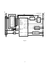
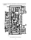
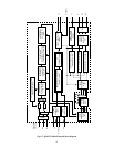
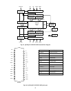
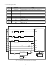
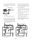
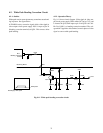
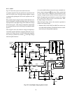
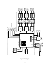
The video/color/deflection section is shown in Fig. 6-2.
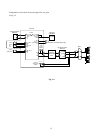
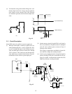
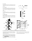
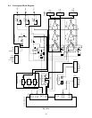
The luminance signal is supplied from pin Y08 of PY01 and
its frequency bandwidth is limited by the low pass filter (LPF)
and then input to pin 36 of V/C/D IC (VIDEO IN). The Y
signal output from pin 12 of PY01 superimposes the charac-
ter signal on the video signal by QY49 and QY44, and then
output to the sub screen process section.
QY49 and QY44 work as the analog switches. When the
screen is displayed in DW, the switch operation is not car-
ried out and the same signal as the input signal is output, and
when the 9-screen multi-search process is carried out, the
switch operation is carried out.
The OSD signal superimposes the shade of character signal
by QY49 and the character signal by QY44 on Y signal.
On the other hand, the color signal is supplied from pin Y15
of PY01, limited its frequency bandwidth by the band pass
filter (BPF) and then input to pin 34 of QY01 (COLOR IN).
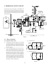
The color difference signals of the demodulated signal (R –
Y) and ( B – Y) are output from pins 13 and 14 of QY01. In
the same way as the Y signal, the (R – Y) and (B – Y) signals
are superimposed on the character signal with OSD signal
by QY44.
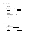
The GBR matrix circuit which converts the Y, R – Y and B –
Y signals into three primary color signal of G, B and R is
used to convert the (R – Y) and (B – Y) signals into I and Q
signals.
In the GBR matrix circuit, each G, B and R output is output
as G – Y, B – Y and R signals when the Y signal is not input.
Then the B – Y signal is converted to Q signal, R – Y to I
signal pseudically by turning the phase by an angle of 33°.
Thus, R – Y and B – Y signals are input to pins 18 and 19 of
QY01, and the output signals from pins 23 and 24 are devel-
oped as the I and Q converted signals pseudically. The am-
plitude of the signals is amplified by 6 dB amplifier of QY23
and the signals are output to the sub screen process section.
Since the sync signal is added to the luminance signal, the
signal is input to pin 39 of QY01 (SYNC SEP IN) and the
sync signals of HD and VD are output to pins 10 and 11 of
QY01. The HD signal is waveshaped by QY42.
The HD signal (WHD1, WHD2) is used as the horizontal
pulse for sub screen write and the VD signal (WVD) is as the
vertical pulse for sub screen write in the sub screen process
section.
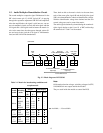
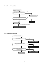
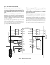
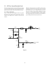
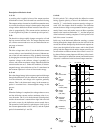
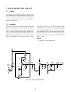
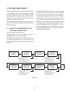
In the sub screen microcomputer section, various kinds of
control signals (brightness, density, hue, etc.) are output from
the sub screen control microprocessor QY91 and the signals
are used for the level matching adjustment. So the setting for
the sub screen cannot be made by the user. Furthermore, the
OSD signal for OSD superimposing is output.
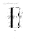
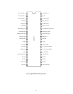
The sub screen process IC control program is stored in the
nonvolatile memory of the sub screen control microproces-
sor QY91 in order to control the sub screen process IC
(TC9092AF), and the data is sent via I
2
C bus.