


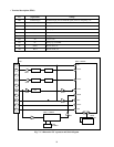
62
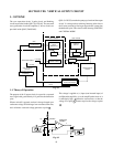
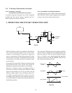
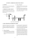
(4) To decrease the collector loss of Q3, the power supply
voltage is decreased during scanning period as shown
in Fig. 8-7, and VCE1 decreases and the collector loss
of Q3 also decreases.
Fig. 8-7 Output stage power supply voltage
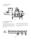
(5) In this way, the circuit which switches power supply
circuit during scanning period and flyback period is
called a pump-up circuit. The purpose of the pump-up
circuit is to return the deflection yoke current rapidly
for a short period (within the flyback period) by ap-
plying a high voltage for the flyback period. The basic
operation is shown in Fig. 8-8.
Q3 Collector loss decreases
by amount of this area
Power supply
for flyback period (Vp)
Power supply
for scanning period
(Vcc)
Scanning period
Flyback period
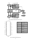
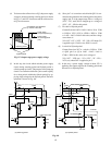
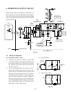
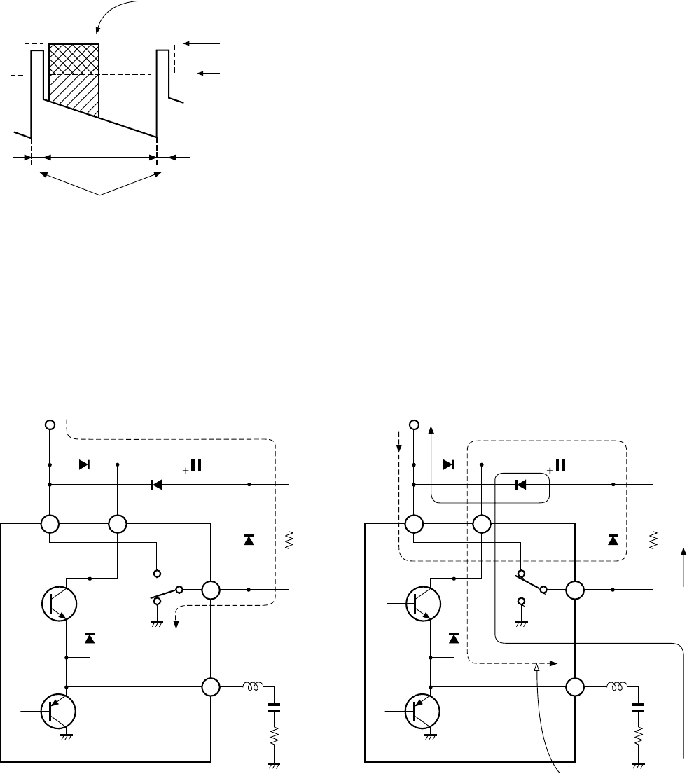
(6) Since pin 7 of a transistor switch inside Q301 is con-
nected to the ground for the scanning period, the power
supply (pin 3) of the output stage shows a voltage of
(VCC – VF), and C308 is charged up to a voltage of
(VCC – VF – VR) for this period.
(7) First half of flyback period
Current flows into L462 + L465 + L464 ® D1 ® C308
® D308 ® VCC (+35V) ® GND ® R305 ® C306
® L462 + L463 + L464 in this order, and the voltage
across these is:
VP = VCC + VF + (VCC – VF – VR) + VF about 63V
is applied to pin 3. In this case, D301 is cut off.
(8) Last half of flyback period
Current flows into VCC ® switch ® D309 ® C308
® Q301 (pin 3) ® Q3 ® L462 + L463 + L464 ®
C306 ® R305 in this order, and a voltage of
VP = VCC – VCE (sat) – VF + (VCC – VF – VR) –
VCE (sat), about 56V is applied to pin 3.
(9) In this way, a power supply voltage of about 35V is
applied to the output stage for the scanning period and
about 63V for flyback period.
6
3
7
2
6
3
7
2
D301 C308
D308
Q301
D309
Switch
Q3
Q4
D1
L462+L463+L464
C306
R305
D301 C308
Q301
D309
Q3
Q4
D1
L462+L463+L464
C306
R305
Switch
VR
Last half
(a) Scanning period (b) Flyback period
First half
+
D308
+
R308
R308
Fig. 8-8