


57
2-2. Circuit Description
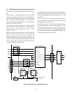
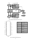
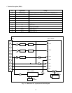
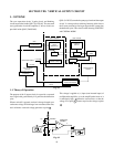
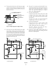
Fig. 7-1 shows a block diagram of the YCS circuit.
(1) A video signal sent through the AV switching circuit
passes the input terminal (DG) and enters the YCS unit.
(2) The video signal entered is limited in its band width in
passing through an aliasing distortion elimination LPF
consisting of LZ22, etc. , and then enters pin 56 of
QZ01.
(3) At the same time, a fsc (3.58 MHz) signal being oscil-
lated in the video signal color IC (Q501, AN1222AN)
is fed to pin 28 of QZ01 and converted into a 4fsc
(14.32 MHz), a drive clock frequency inside the IC.
(4) The video signal entered pin 56 of QZ01 is processed
inside the IC and a luminance (Y) signal is developed
at pin 48 of QZ01 and the color signal at the pin 51.
(5) The Y signal developed at pin 48 of QZ01 passes a
LPF (LZ20, etc.) which eliminates the clock signal
component, amplified by a 6dB amplifier QZ21, etc.
and comes out from the DC terminal as the Y signal.
(6) At the same time, the color signal developed at pin 51
of QZ01 passes a LPF (LZ21, etc.) which eliminates
the clock component, amplified by 6dB by QZ23, etc.
and comes out from DD terminal through a buffer of
QZ24 as the C signal.
(7) QZ04 is generating a clock signal used to read and
write the digital data between QZ03 and QZ04 based
on the video signal.
(QZ16 emitter: 28.6 MHz ± 0.2 MHz, adjusted by
LZ25.)
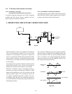
1. OUTLINE
The 3D YC separation circuit uses a comb filter with a frame
memory and ideally separates the Y (luminance) and color
signal for still parts of a picture, thus providing a clean pic-
ture without:
(1) Dot interference causing at border areas of color pic-
tures.
(2) Excess color in vertical direction.
However in a moving picture, as the picture moves between
the first and second frames, good separation is not obtained.
To prevent this, a motion detection is carried out in the 3D
YC separation (hereafter called YCS) unit (PB6347). When
a picture moving is detected a 2D YC separation using a
line memory is switched in and when not detected or for a
still picture 3D YC separation is switched in, thereby cor-
recting defects both the systems have and performing the
ideal YC separation. The motion detection accuracy and
smoothness of the switching, etc. are controlled through the
IIC bus.
After completion of the Y and S signal separation, a vertical
contour correction is carried out for the Y signal.
2. CIRCUIT DESCRIPTION
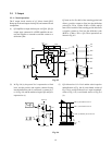
2-1. Configuration
The YCS unit consists of a YC separation IC (QZ01,
TC9086F) which plays major roles, 2 Mbyte field memory
(QZ02, QZ03), clock generation IC (QZ04, TA8667F), and
peripheral circuits (LPF, AMP,emitter followers, etc.).
Of the above circuit blocks, QZ01 (TC9086F) includes an
A/D converter, D/A converter, clamp circuit, 4fsc PLL cir-
cuit, 1 line dot countermeasure circuit, vertical contour cor-
rection logic circuit, etc. and provides a high separation with
less variations.
SECTION VII: 3-DIMENSION Y/C SEPARATOR CIRCUIT