


78
6-1-3. Actual
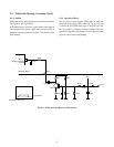
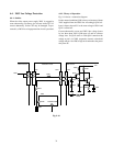
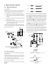
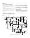
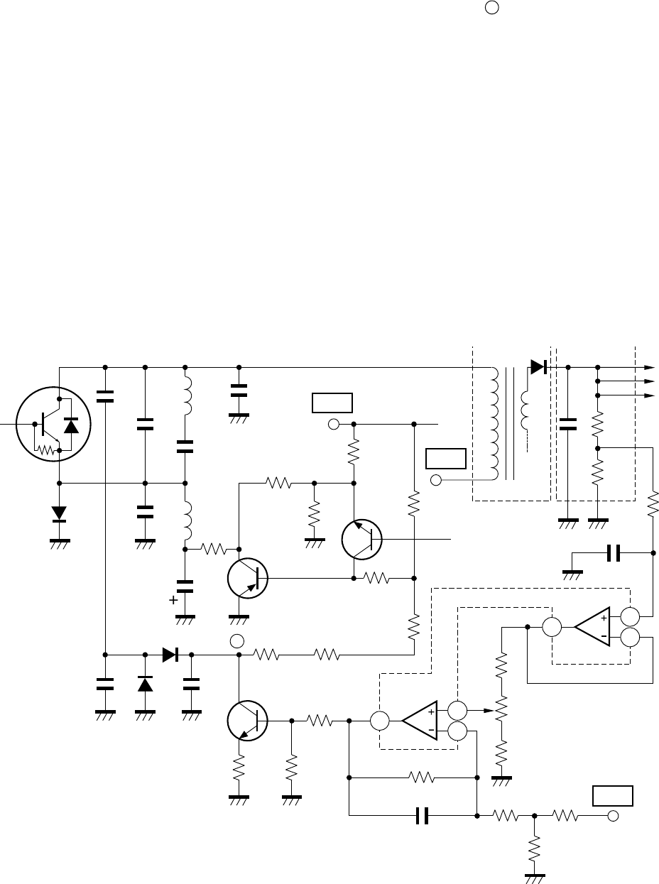
Fig. 9-22 shows the actual circuit used in the unit.
A resonant capacitor C0 is also split into two capacitors C443
and C444 in this circuit. The high voltage regulator cirucits
is structured by splitting the C443 to two capacitors of C443
and C448.
Here, assume a high voltage increases and the detection volt-
age E
D
' obtained by dividing the high voltage also increases
in proportional to the high voltage. This makes the voltage
E
D
increase at pin 7. (The voltage is impedance transformed
by a voltage follower circuit consisting of op amplifier Q483
at pin 7.)
The voltage E
D
and a 9V reference voltage developed by a
3-terminal regulator Q420 are compared. When the E
D
in-
creases, the voltage at pin 2 of Q483 differential amplifier
also increases, and the base current I
B
of the high voltage
transistor Q480 increases.
As a result, Q480 collector current increases and Q480 col-
lector voltage (at the point B ) decreases. Then, a peak value
of V
CP2
across C418 is clamped by the diode D443 at the
collector voltage lowered, and the collector voltage V
CP
of
Q404 (H output transistor) obtained as a sum of the voltage
V
CP1
across C443 and V
CP2
across L418 decreases. Then,
the high voltage also decreases.
When the high voltage lowers, the corrective operation is
carried out in reverse order.
* Resustors R451, R452, R453 and R455 are used to cor-
rect undersirable influence (H amplitude increase at mini-
mum I
H
) by the H amplidude regulator.
Fig. 9-22 Actual high voltage regulator circuit
Horizontal
output
Q404
C443
C444
C
S
L462
L463
L464
D461
C467
L461
R463
C440
-27V
C464
Q460
R466
R461/R469
R460
Q462
R455
125V
R454
R453
R452
R451
B
D443
C418
D444
C419
Q480
R434
R431 R492
2
3
4
R488
C483
R494
R439
R487
Q420
9V-1
8
6
7
E
D
Q483
C482
R435
E
D
'
FBT
E
H
R489
R450
R490
CR-BLOCK