


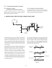
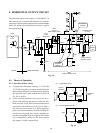
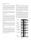
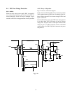
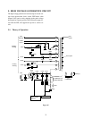
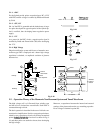
69
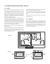
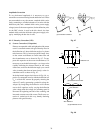
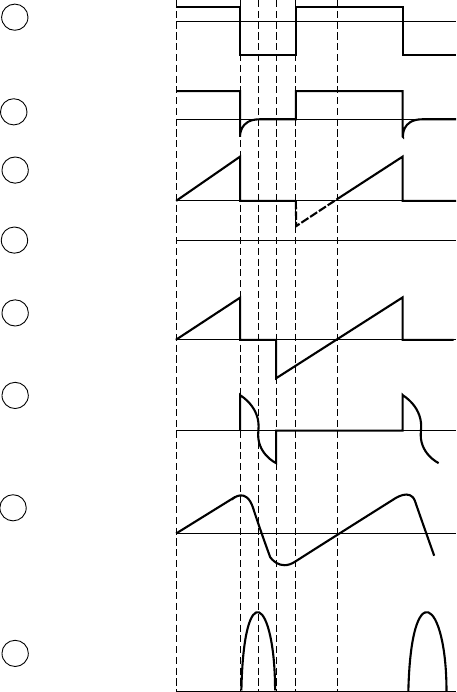
Description of the basic circuit
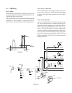
1. t1~t2:
A positive pulse is applied to base of the output transistor
from the drive circuit, and a forward base current is flowing.
The output transistor is turned on in sufficient saturation area.
As a result, the collector voltage is almost equal to the ground
voltage and the deflection current increases from zero to a
value in proportionally. (The current reaches maximum at
t2, and a right half of picture is scanned up to this period.)
2. t2:
The base drive voltage rapidly changes to negative at t2 and
the base current becomes zero. The output transistor turns
off, collector current reduces to zero, and the deflection cur-
rent stops to increase.
3. t2~t3:
The drive voltage turns off at t2, but the deflection current
can not reduce to zero immediately because of inherent na-
ture of the coil and continues to flow, gradually decreasing
by charging the resonant capacitor C0. At the same time, the
capacitor voltage or the collector voltage is gradually in-
creases, and reaches maximum voltage when the deflection
current reaches zero at t3. Under this condition, all electro-
magnetic energy in the deflection coil at t2 is transferred to
the resonant capacitor in a form of electrostatic energy.
4. t3~t4:
Since the charged energy in the resonant capacitor discharges
through the deflection coil, the deflection current increases
in reverse direction, and voltage at the capacitor gradually
reduces. That is, the electrostatic energy in the resonant ca-
pacitor is converted into a electromagnetic energy in this
process.
5. t4:
When the discharge is completed, the voltage reduces to zero,
and the deflection current reaches maximum value in re-
verse direction. The t2~t4 is the horizontal flyback period,
and the electron beam is returned from right end to the left
end on the screen by the deflection current stated above.
The operation for this period is equivalent to a half cycle of
the resonant phenomenon with L and C0, and the flyback
period is determined by L and C0.
6. t4~t6:
For this period. C0 is charged with the deflection current
having opposite polarity to that of the deflection current
stated in "3.", and when the resonant capacitor voltage ex-
ceeds VCC, the damper diode D conducts. The deflection
current decreases along to an exponential function (approxi-
mately linear) curve and reaches zero at t6. Here, operation
returns to the state described under "1.", and the one period
of the horizontal scanning completes. For this period a left
half of the screen is scanned.
In this way, in the horizontal deflection scanning, a current
flowing through the damper diode scans the left half of the
screen; the current developed by the horizontal output tran-
sistor scans the right half of the screen; and for the flyback
period, both the damper diode and the output transistor are
cut off and the oscillation current of the circuit is used. Us-
ing the oscillation current improves efficiency of the circuit.
That is, about a half of deflection current (one fourth in terms
of power) is sufficient for the horizontal output transistor.
Fig. 9-6
A
B
C
D
E
F
G
H
t1 t2 t3 t4 t5 t6
0
0
0
0
0
0
0
0
TR
base voltage
TR
base current
TR
collector
current
D
damper
current (SW2)
Switch
current
(TR, SW1)
Resonant
capacitor
current (Co)
Deflection
current (Lo)
TR
collector
voltage