Process control
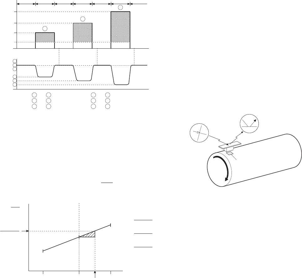
1 Toner patch images are formed on the photoconductor surface
under the three process conditions (MC grid bias voltage).
At the first process control, a toner parch image is formed with the
reference grid voltage –410V as the center and ±30V. At the
second or later process control, the MC grid bias voltage deter-
mined at the former process control is used as the center, and a
toner patch is formed under the process condition of ±32V to the
center value.
2 Measure the three toner patch images formed in the above and
the drum surface with the process density sensor to obtain the
relations.
BVS: Sensor detection level on the photoconductor drum surface
PVS: Sensor detection level with the toner patch image
Obtain the above two levels from the calculation formula and record
them as the reference values.
A. STD BA: Reference level when detecting the drum surface
→ STD BA = BTS x 20
B. STD PA: Reference level when detecting the toner patch image
→ STD PA = PTS x 20
In the density correction, the process conditions are determined
so that the ratio of the reference levels
STD PA
STD BA
set in the above
may be maintained at constant.
3 Obtain the MC grid bias voltage from the reference level ratio.
In the SF-2214/2118, the absolute value of the output of the den-
sity sensor is not directly used for control calculation, but the ratio
of the sensor output value (BA) on the drum surface and the
sensor output (PA) of the toner patch image is used for control
calculation.
* The grid bias value is obtained so that the ratio of the drum
surface level and the sensor level when forming patch level and
the sensor level when forming patch images is 200:40.
Though, therefore the light quantity of the reflection type sensor is
varied by dirt or deterioration, the ratio (PA/PB) will not be affected
by change in light quantity to provide stable control.
The grid voltage value where the same density level as the refer-
ence level is obtained is displayed by Sim. 44-9 "a". This value is
displayed with 50 as the center in the range of 0 ~ 99 in integer
numbers. The correction for 50 is 0V (–410V), and the correction
for 58 is +30V (–442V).
4 When the MC grid bias voltage is corrected by the process con-
trol, the corresponding light quantity is calculated to control the
copy lamp.
To correct the MC grid voltage, the delta value of the sensitivity
level when the initially recorded reference grid voltage is –440V
and the MC grid voltage where the same density is obtained in
process control is fed back to the MC grid voltage of each mode.
Process control timing
In the SF-2035, the process control is performed in the following
timing:
1 When the main switch is turned on and the first copy is made:
2 At every specified copy quantity (First copy after 1,000 copies)
Judged by the total counter.
The correction is reset by Simulation 25-2.
3 After the specified time after turning on the main switch. (First
copy after 44, 60, 120, 180 min)
Drum marking
In this model, a toner patch image is formed in the same position on
the photoconductor drum surface to improve the accuracy of the
process control.
A marking is provided on the drum and the marking is sensed before
forming a toner patch image. If the marking level is not sensed, the
developing lamp blinks and the trouble code (F2-32) is displayed.
Basic structure
Photoconductor drum: The 65mmφ ground plate of the OPC
drum is on the rear frame side of the drum
unit so that it contacts the drum locator
pin.
Blank lamp: The non-image area is exposed by the
light from the blank lamp to erase the
positive potential outside the drum CTL.
Use of the latchet simplifies the lamp posi-
tion adjustment.
Discharge lamp: Eight bulbs cast light over the drum sur-
face to erase the positive potential in CTL.
Ventilation hole provided in the drum
frame releases heat from bulbs.
Cleaning mechanism: The cleaning blade removes the toner
remaining on the drum surface. The blade
always rests on the drum surface.
Main corona: The saw teeth corona charge method is
used. Use of the screen grid maintains the
even charge potential over the photocon-
ductor surface.
Enforced separation
mechanism:
Using two pieces of separation pawl, the
copy paper stuck over the drum surface is
forced to separate from the drum surface.
472V
BV
PV
Bias
440V
408V
1
2
3
1
2
3
1ID PAT =P V 1 x 20
2
I DPAT = PV 2 x 20
3
I DPAT = PV 3 x 20
1
IDBAS =BV 1 x 20
2
IDBAS =BV 2 x 20
3
IDBAS =BV 3 x 20
Drum 1/2 rotation 2/2 rotation 3/2 rotations
Surface
Toner
image Surface
Toner
image Surface
Toner
image
1
2
3
Surface
1=
ID PAT1
ID BAS1
2=
ID PAT2
ID BAS2
3=
ID PAT3
ID BAS3
PA
BA
-440-410-380
3
2
1
STD PA
STD BA
GB PAT
( ӊ)
MC grid bias voltage
R
F
6mm x 7mm
5 – 15


