171
8.2 Register of Programmable Pulse Generator (PPG0, 1)
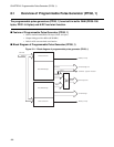
The register configuration/functions of the programmable pulse generator (PPG0, 1) are
described.
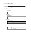
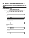
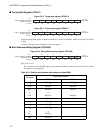
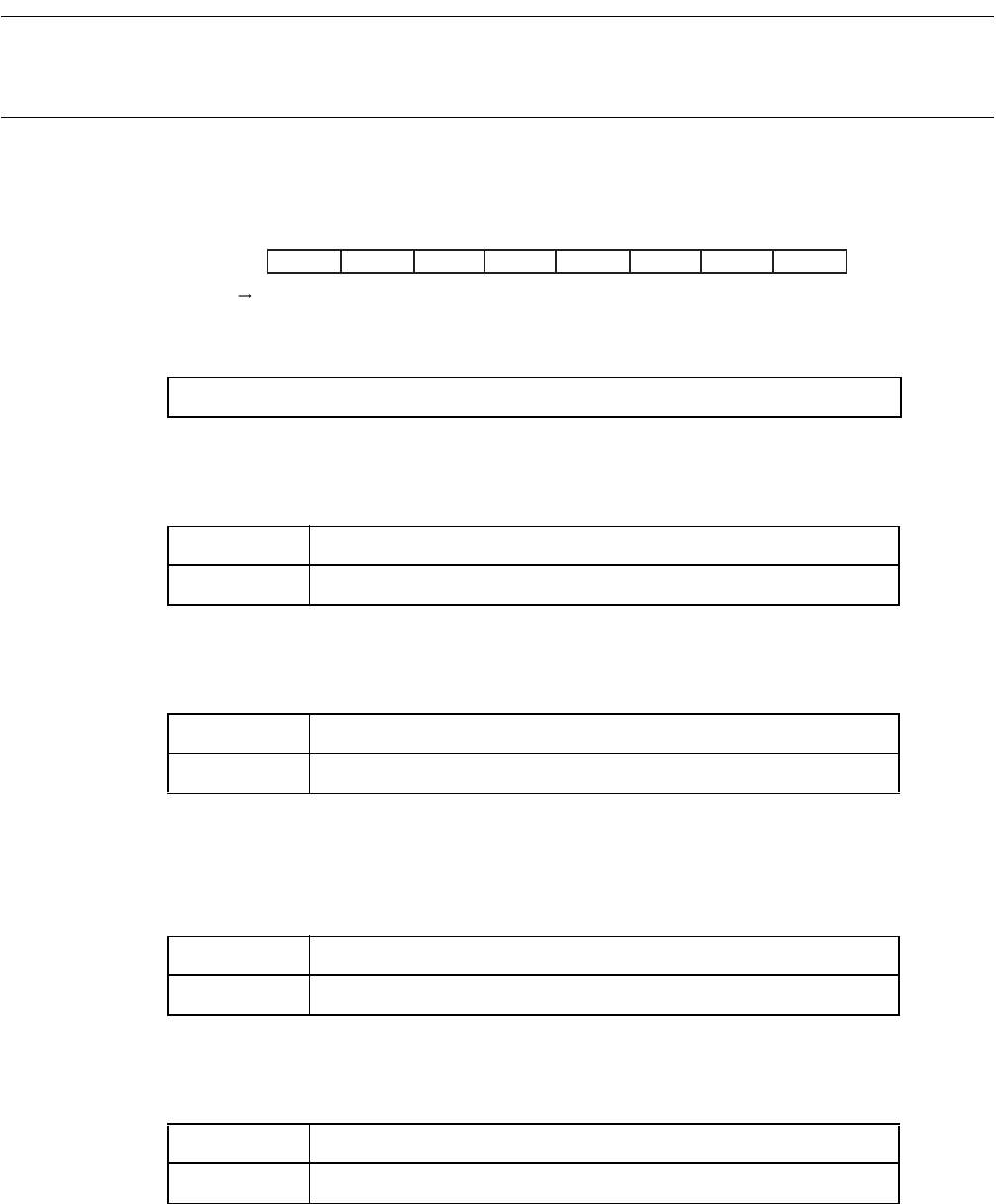
■ PPGx Control Register (PPGxC)
Figure 8.2-1 PPGx control register (PPGxC)
[bit7 to 4]:Test
[bit3]:IF
It is output timing data match interrupt request flag.
[bit2]:FCLR
It is interrupt request flag clear bit.
The read value of this bit is always "1".
[bit1]:IE
It is interrupt enable bit.
[bit0]:ST
It is PPG start bit.
7 6 5 4 3 2 1 0
0000 X100
B
Initial value
bit
Address: 0003C0
H
(PPG0C)
0003C4
H
(PPG1C)
R/W R/W R/W R/W R/W R/WRW
Test Test Test Test IF FCLR IE ST
Access
Please set "0".
0 Not match
1 Match
0 Clear IF.
1 None
0 Interrupt interdiction
1 Interrupt permission
0 PPG stop
1 PPG start


