80
CHAPTER 3 CPU
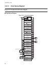
3.12.11 Clock Series Diagram
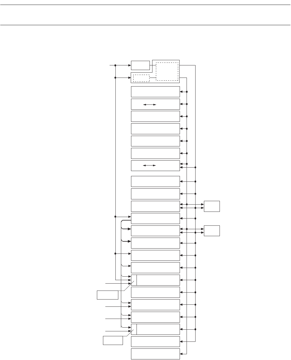
Figure 3.12-14 shows the clock series diagram.
■ Clock Series Diagram
Figure 3.12-14 Clock series diagram
Clock
generation
unit
φ
θ
XO
CFG,DFG,FRG0-1
PCK
EC4
EC5
PLL
1/2
CPU
I/D
C bus
convert
R bus
convert
ROM
RAM
Custom
External bus control
D
RAM
RAM
Interrupt control
A/DC
SIO to 2
FRC
PPG0 to 1
RTG0 to 2
PWM0x to 1x
PWC
FG input unit
Ext-INT
General - purpose
Prescaler
Timer 0 to 4
Timer 5
General - purpose
port C to D
General - purpose
port 0 to 7
Sync with X0
Sync with φ


