


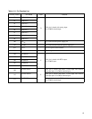
9
1.5 Pin Function Description
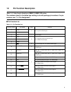
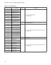
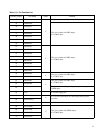
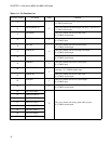
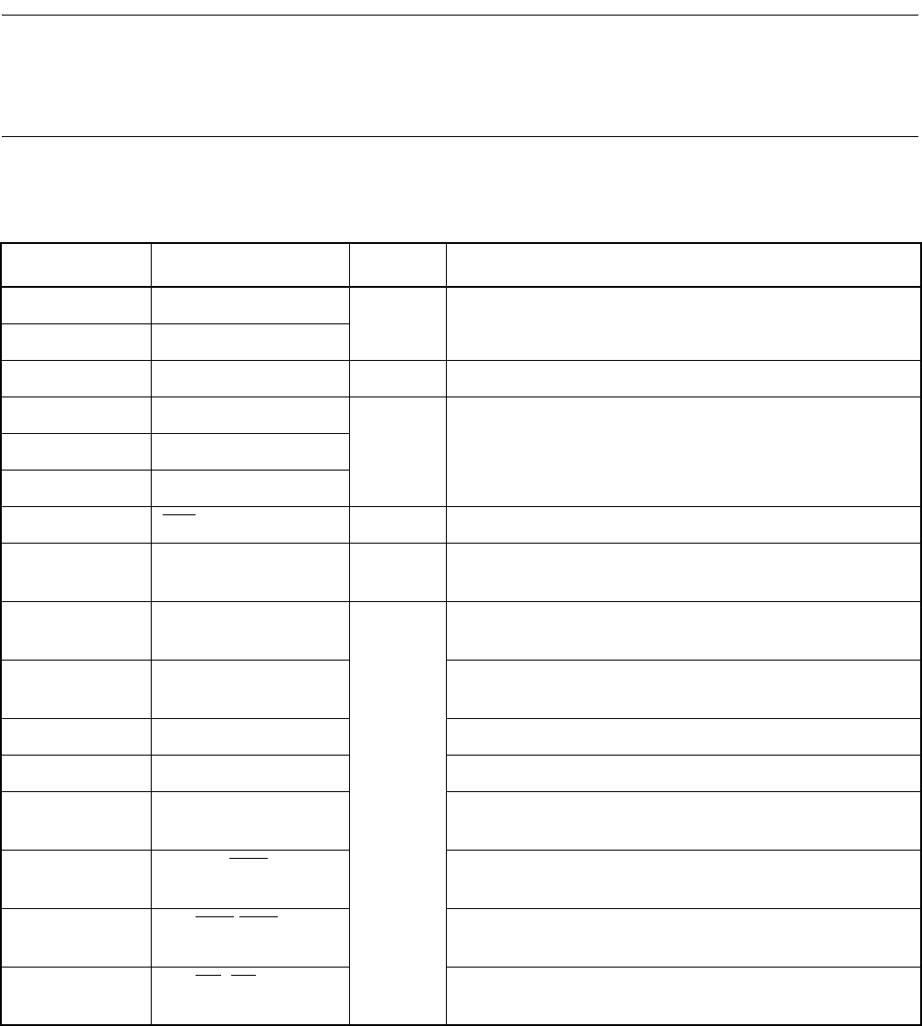
Table 1.5-1 lists the pin function of MB91191/MB91192 series.
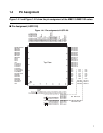
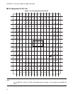
The numbers shown in the tables has nothing to do with package pin numbers. For pin
numbers, see "1.4 Pin Assignment".
■ Pin Function List
Table 1.5-1 Pin Function List
Pin No. (LQFP) Pin name Form Function
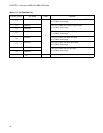
1 X0(I)
A It is crystal oscillation pin.
2 X1(O)
3 Vss - It is Vss pin.
4 MD2
B
It is operating mode specification pin.
It is CMOS schmitt input.
5 MD1
6 MD0
7 RST
B It is reset input pin. It is CMOS schmitt input.
8
P70/XOUT
C
This pin is shared with clock output (X0/2, PCK/2). It is
CMOS input.
9
P67/T4O
C
This pin is shared with timer 4 square wave output. It is
CMOS input.
10
P66/T5O1 This pin is shared with timer 5 square wave output. It is
CMOS input.
11 P65 It is general-purpose I/O port. It is CMOS input.
12 P64 It is general-purpose I/O port. It is CMOS input.
13
P63/ALE/ALE This pin is shared with address strobe output.
It is CMOS input.
14
P62/P62/WR1
This pin is shared with write strobe output 1.
It is CMOS input.
15
P61/WR0
/WR0 This pin is shared with write strobe output 0.
It is CMOS input.
16
P60/RD
/RD This pin is shared with read strobe output.
It is CMOS input.