144
CHAPTER 6 FG Input
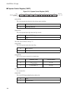
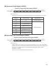
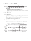
■ Capstan Control Register (CAPC)
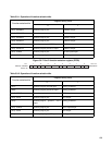
Figure 6.2-3 Capstan Control Register (CAPC)
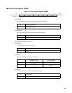
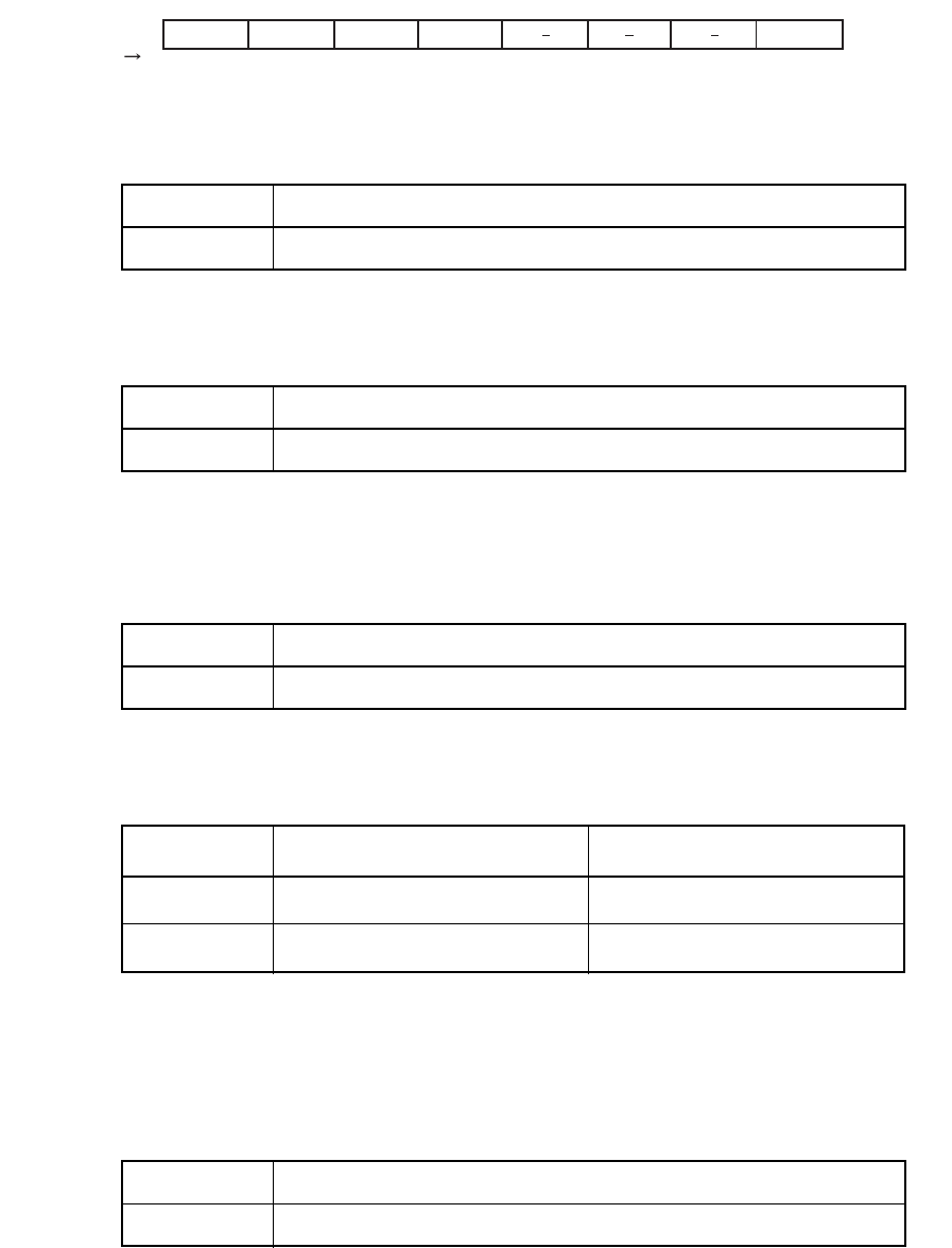
[bit7]:CFGD
This is the capstan edge detection flag during capstan masking.
[bit6]:FCLR
This is the capstan input edge detection flag clear bit.
The read value of this bit is always "1".
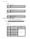
[bit5]:CMTS
This is the capstan mask timer status flag.
[bit4]:MTCS
This is clock source selection bit of mask timer.
[bit3 to 1]:
It is an unused bit.
[bit0]:DUB
This is the CFG input multiplication selection bit.
7 6 5 4 3 2 1 0
X1X0 ---0
B
Initial value
bit
CFGD FCLR CMTS MTCS DUB
RWR
R/W
Access
Address: 000052
H
0 Without edge detection
1 With edge detection
0 Clear the CFGD flag.
1 None
0 Mask released
1 Masking
Selection Clock in fch:@20MHz
0
2
10
/fch (FRC9)
51.2 µs
1
2
14
/fch (FRC13)
819.2 µs
0 None
1 2 multiplication


