281
■
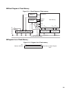
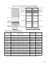
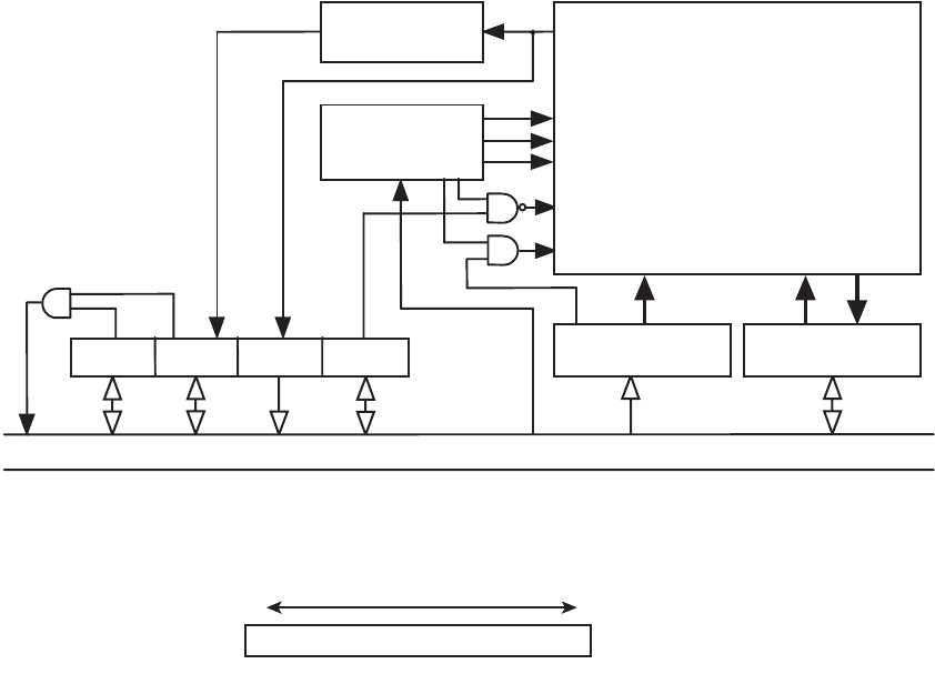
Block Diagram of Flash Memory
Figure 21.1-1 Block Diagram of Flash memory
■
Register List of Flash Memory
Figure 21.1-2 Register list of Flash memory
INTE
Interrupt request
Bus control
signal
RDYINT RDY WE
FR-C Bus (Instruction/Data)
Address buffer Data buffer
Control signal
generation
Rasing edge
detection
Flash Memory
CEX
WEX
OEX
BYTEX
FA
18 to 0
DI
15 to 0
DO
31 to 0
RESETX
RDY/BUSYX
CA
18 to 0
CD
31 to 0
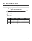
7 0
Flash Memory Status Register
bit
FSTR
(4bit)
Address: 0007C0
H


