


4
CHAPTER 1 Overview of MB91191/MB91192 Series
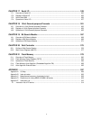
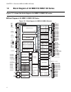
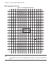
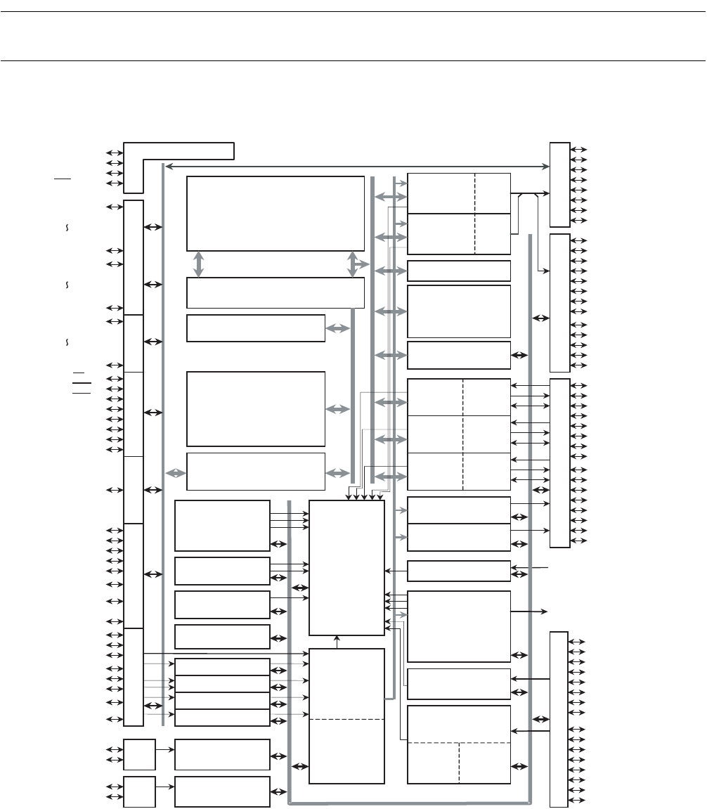
1.2 Block Diagram of All MB91191/MB91192 Series
Figure 1.2-1 shows the block diagram of all MB91191/MB91192 series.
■ Block Diagram of All MB91191/MB91192 Series
Figure 1.2-1 Block diagram of all MB91191/MB91192 series
PC2/PWM 12/SCS1
PC3 /PWM11/SCS2
PC4 /PWM10
PC5 /PWM02
PC6 /PWM01
PC7 /PWM00
PD4 /SO1
PD5 /SCK1
PD6 /SCS0
PD7/SI0
PC0/SO0
PC1/SCK0
PD3 /SI1 /INT 2
PD1 /SO2
PD2 /SCK2
PD0 /SI2
PA7/AN-F/KEY7
PA4/AN-C/KEY4
PA3/AN-B /KEY3
PA2/AN-A /KEY2
PA1/AN-9 /KEY1
PA0/AN-8 /KEY0
PB7/AN-7
PB6/AN-6
PB5/AN-5
PB4/AN-4
PB3/AN-3
PB2/AN-2
PB1/AN-1
PB0/AN-0
INT2-0 (from por t1,D )
OSCI
OSCO
XO
X1
P80/PPG04
P94/PPG03
P93/PPG02
P92/PPG01
P91/PPG00
P90/PO
P87/PPG11
P46/PPG18
P40/PPG12
P47
P06/EXI1
P05/EXI 0
P01/RFG0
P00/RFG1
P03/DFG
PO2/DPG
P07/EXI 2/PMI
P04/CFG
P10/PMSK
P11/EC4/INT0
P12/EC5/INT1
PA6/AN-E/KEY6
PA5/AN-D/KEY5
RTO4-0 (t o port 1)
P16/RTO3
P17/RTO4
P14/RTO1
P15/RTO2
P13/RTO0
P70/XOUT
P65
P64
P67/T4O
P66/T5O1
P61/WR0
P60/RD
P63/ALE
P62/WR1
P50/A08
P57/A15
P20/D16
P27/D23
P30/D24
P37/D31
MD1
MD0
RST
MD2
P86/PPG10
P85/PPG09
P84/PPG08
P83/PPG07
P82/PPG06
P81/PPG05
P41/PPG13
P42/PPG14
P43/PPG15
P44/PPG16
P45/PPG17
I-bu s D-bus
I-bu s D-bus
D-bus R-bus
C-bus
P
O
R
T
P
O
R
T
P
O
R
T
P
O
R
T
P
O
R
T
P
O
R
T
P
O
R
T
P
O
R
T
P
O
R
T
2
/
3
5
6
7
1
0
4
8
/
9
C
/
D
P
O
R
T
A
/
B
Mode Control
FR20 CPU Core
RAM 2KB
MB91191R : ROM 254KB
MB91192 : ROM 384KB
MB91F191A: FLASH 254KB
MB91F192 : FLASH 384KB
External Bus CTL
16bit Timer0-3
8/16bit Timer
16bit Timer4
8bit PWC
CFG
DFG
RFG0
RFG1
OSC
OSC
C-unit
10bit Programale
Prescaler
Interrapt
Controler
24bit FRC
fifo
29bit x 8
RAM 256Byte
RAM 64Byte
PPG0
PPG1
Bit Search
MB91191R :RAM 6KB
MB91192 :RAM 8KB
MB91F191A:RAM 6KB
MB91F192 :RAM 8KB
RAM
128Byte
RAM
128Byte
RAM
128Byte
Serial
ch0
Serial
ch1
Serial
ch2
12bit PWM00-02
12bit PWM10-12
External-Interrapt
16bit RTGO-2
External-Interrapt
(Key input)
10bit A/DC
fifo
(soft)
fifo
(hard)