22
CHAPTER 2 Handling Devices
2.2 Others
The others are explained
■ External Reset Input
When "L" level is input to the RST pin, to ensure the inside achieves reset status, "L" level input to the
RST
pin is required for at least five machine cycles.
■ Note on Using External Clock
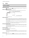
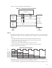
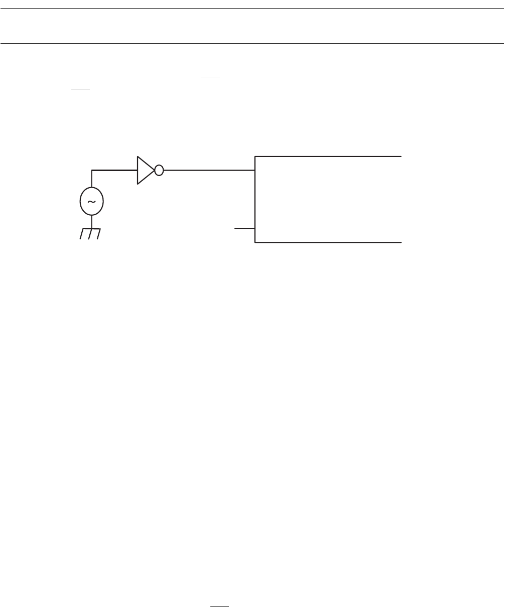
When using the external clock, drive the X0. Figure 2.2-1 shows the example of using an external clock.
Figure 2.2-1 Example of using an external clock
*:Be sure to make X1 pin open.
■ Power Supply Pin
If there are multiple V
DD
and V
SS
pins, from the point of view of device design, pins to be of the same
potential are connected the inside of the device to prevent such malfunctioning as latch up. To reduce
unnecessary radiation, prevent malfunctioning of the strobe signal due to the rise of ground level, and
observe the standard for total output current, be sure to connect the V
DD
and V
SS
pins to the power supply
and ground externally.
Also try to ensure that connection to the V
DD
, Vss on this device is at the lowest impedance possible from
the power supply source. In addition, We will recommend the ceramic capacitor of about 0.1 µF to be
connected as bypass capacitor between V
DD
and V
SS
near this device.
■ Crystal Oscillation Circuit
The noise near X0 and the X1 terminal becomes original of the malfunction of this device. The printing
board should be designed so that the X0, X1, crystal oscillator (or ceramic oscillator), and bypass capacitor
to the ground are arranged as close as possible.
Printing board artwork around the X0 and X1 terminals to the ground is strongly recommended, as steady
operation can be expected.
■ Handling NC Pin
Use the Non Connect (N.C.) terminal while open.
■ Mode (MD0 to MD2) Pin
Please tie directly to V
DD
or V
SS
and use these terminals.
In order to prevent erroneous entry to test mode due to noise, the pattern length between each mode
terminal and V
DD
or V
SS
on the printing board should be as short as possible, and they should be connected
at low impedance.
■ At Power On
When the power is turned on, the RST pin must be started from "L" level status, and changed to "H" level
after at least five cycles of the internal operation clock have passed, after the power source reaches the V
DD
level.
MB91191/MB91192 series
X0
X1
OPEN


